|
August 1945 Radio-Craft
 [Table
of Contents] [Table
of Contents]
Wax nostalgic about and learn from the history of early electronics.
See articles from Radio-Craft,
published 1929 - 1953. All copyrights are hereby acknowledged.
|
This is the first of a three-part
series on radio detector circuits by Mr. Robert Scott. It appeared in the August
1945 issue of Radio-Craft magazine. He begins in this article with describing
diode action and progresses to uses in various types of signal detectors in radio
receivers. A discussion of modulation and distortion sources is included as well.
The strange-looking round schematic symbols are vacuum tubes, which used metallic
elements separated by space as functional elements rather than fused sand containing
traces of impurities. Don't be intimidated, though; just think of them as field
effect transistors (FETs) where the plate is the drain, the grid is the gate, and
the cathode is the source. The next article in the series discusses hi-fidelity
triode detectors; the plate rectifier, infinite-impedance detectors, grid rectification,
and regenerative circuits.
Part I
appeared in the August 1945 issue, Part II in
September, and Part III,
the final article in the series, was published in the
October edition.
Detector Circuits
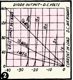
Fig. 2 - Characteristic chart for diode tube.
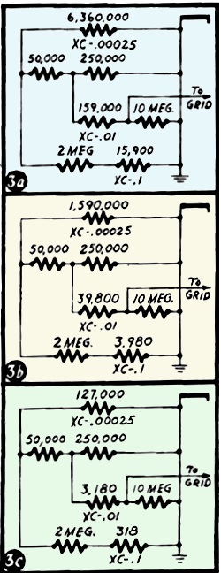
Fig. 3 - Diode action at three frequencies.
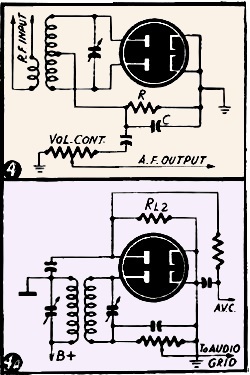
Fig. 4 - Full-wave detector. 4a - Detector and A.V.C. circuit
for minimum distortion.
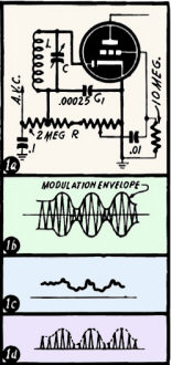
Fig. 1 - Circuit of a typical diode detector.
Part I - The Diode Detector.
By Robert F. Scott
A detector has been described as a means of separating speech or other intelligence
components from a radio frequency carrier signal. Detection or "demodulation" is
necessary for practically every type of communication which utilizes a basic carrier
signal of a frequency well above the audio scale.
There are several methods of separating the intelligence from the carrier. Each
of these has its own particular advantages and disadvantages which will be discussed
in turn. The most important of these traits are: Sensitivity, Fidelity, Signal handling
capacity, and Circuit loading.
Sensitivity of a detector is its ability to respond to comparatively weak signals
and this ability is measured as the ratio of R.F. signal input to audio signal output.
Fidelity is the ability to handle audio signals without discrimination against
frequency or amplitude. Thus a high fidelity detector will give faithful reproduction
of the intelligence envelope of the modulated signal.
Signal handling ability of the detector is its ability to handle signals varying
from maximum to minimum signal strength without deleterious effects from insufficient
input voltage and overloading.
The circuit loading is the load which the detector circuit imposes upon the preceding
stage. It is this factor which must often be carefully calculated; because a low
impedance often means that the detector will draw current, and not all preceding
stages are designed to furnish the driving power.
The Diode Detector Circuit
Perhaps the simplest and most often used detector is the diode. This employs
a tube having only a cathode and anode or plate. Fig. 1-a illustrates a typical
diode detector circuit as commonly employed in the receivers of today. A grid and
triode plate are included in many such tubes, but play no part in the detector action.
Figs. 1-b-c-d show the shape of the modulated input signal, condenser charging voltage
and diode current flow respectively.
The modulated signal voltage is applied to the combination of L-C and hence between
(diode) plate and cathode of the detector tube. It is well-known that the plate
attracts electrons (or draws current) only when it is positive with respect to the
cathode. As the input signal increases from zero in a positive direction, the plate
is charged positively and electrons flow from the cathode, resulting in a current
flow. This current flow passes through the load resistor, R, and there is a voltage
drop across this resistor. The voltage across this resistor will be a replica of
the positive halt of the modulated input signal. Condenser C1, will take on a charge
equal to the voltage across R which is slightly less than the peak voltage of the
input cycle.
On the negative portion of the input cycle, the plate is negative with respect
to cathode and there will be no current flow. This current flow is also prevented
by the presence of the negative charge on the plate of the condenser which is connected
to the plate through the L-C network. For the current to commence to flow, it is
necessary for the peak charging voltage to exceed the, voltage on the condenser
for the voltage on the plate, for subsequent cycles will be the algebraic sum of
the voltage on the condenser and the peak charging voltage.
In this manner, the effects of the R.F. will be removed from the output and the
voltage across R will constantly follow the shape of the modulating envelope.
For the highest detector efficiency or sensitivity, it is necessary that the
value of R be made as high as practical when compared with the value of plate resistance.
The ratio of Rp to R may be made from 20 to 100 for efficiencies from
80 to 95 per cent.
Use of Characteristic Curves
The average vacuum-tube manual will supply the characteristic curves of the diode
detector when sine-wave voltages are applied to the input circuit with various values
of load resistances. The conditions demonstrated in these charts demonstrate only
the static characteristics of the tube, but are helpful in determining the dynamic
conditions under which it will operate most efficiently. Due to many factors, the
detector will react very differently from its static characteristics when it is
fed the complex wave forms of speech or music. Even casual study indicates that
the highest values of output voltage will be available with the highest values of
load resistance. Such a chart is shown in Fig. 2.
The circuit in Fig. 1-a shows the second detector of a popular A.C. receiver
using a 12SQ7 tube as half wave rectifier or detector, A.V.C. and first audio stage.
It will be noted that in this circuit, the diode load consists of two resistances
having a total resistance of .3 meg. 250,000 ohms of this resistance is employed
as the volume control for the receiver. The .00025 condenser is used to filter out
the pulsations which would result from the R.F. in the circuit. The direct current
flowing through the load resistance is also tapped off to supply negative automatic
volume control voltage for the I.F. stages of the set.
Figures 3-a-b-c show equivalent circuits at 100, 400 and 5000 cycles. At various
audio frequencies, the reactance of the various condensers will change inversely
as the frequency (as the frequency increases, reactance decreases). The principal
offender of the high frequency shunting is the by-pass condenser, C1. Its reactance
at 100 cycles is almost six and one half megohms. This value of reactance shunting
300,000 ohms will have negligible effect on the audio output at this low frequency.
At 400 cycles the audio output will be still lower and at 5,000 cycles, the reactance
of the R.F. by-pass condenser is 127,000 ohms. When we consider this value paralleling
the load resistance of 300,000 ohms we have an equivalent resistance of only 89,227
ohms. Then, considering the A.V.C. resistor and the grid leak in parallel with the
load resistance, even this value will be lowered somewhat.
High Modulation Percentages
It has been stated that the voltage drop across the load resistance is somewhat
lower than the peak charging voltage. Now, if the resistance offered to the flow
of A.C. is less than that offered to the flow of D.C. then the current caused by
the flow of A.C. will be greater than that caused by the D.C. When the shape of
a modulated signal is studied, it will be noted that as the modulation percentage
approaches one-hundred per cent the instantaneous current flowing through the diode
becomes smaller and reduces to zero at maximum modulation. When the diode input
contains signals having high modulation percentages and containing high frequencies,
the R.F. by-pass condenser cannot dissipate its charge through the load resistor
fast enough to follow the shape of the modulation envelope. Thus there will be frequency
and amplitude distortion.
To determine the value of the R.F. by-pass condenser, the highest modulation
frequency to be received will have to be considered as well as the inter-electrode
capacity of the tube and the broadcast frequencies to be covered by the receiver.
If its reactance is from 2 to 3 times the load resistance at the highest modulation
frequency, then it will be possible to receive signals which have been modulated
up to 94 per cent without distortion. Higher modulation peaks may be received without
distortion becoming noticeable. However, the reactance of this condenser should
be as small as possible, because for maximum output from the detector, it is necessary
for the maximum R.F. voltage to be applied to the diode plate. If the reactance
of the condenser is fairly large compared to the load resistance, a large percentage
of the R.F. voltage will be lost across it. It is for this reason that the diode
detector is seldom employed for low frequency receivers.
Some Causes of Distortion
The shunting effect of the various condensers and resistances in the circuit
has the effect of reducing the effective load resistance of the tube. The dynamic
load line of the tube's characteristic curve will pass through the operating point
but will have a slope such that it will have a cut-off characteristic at an input
voltage less than zero and the distortion will be severe at modulation percentages
where the instantaneous current approaches zero. Theoretically, the diode would
not be able to handle successfully a signal having a high degree of modulation,
but fortunately there is another factor that serves to nullify this effect.
It has been found that the maximum degree of modulation that can be placed upon
an R.F. signal and be detected by the diode without distortion is equal to the equivalent
impedance at the highest modulation frequency divided by the diode load resistance.
When the efficiency of the detector is high, the load resistance offered to R.F.
is equal to the load resistance, R, divided by the efficiency. Since the impedance
is lower for A.C., the resistance offered to A.C. is equal to the effective resistance
divided by the efficiency. The modulation percentage will therefore apparently be
reduced and the distortion produced by the diode in the actual detection of highly
modulated signals cut down.
The tubes selected for diode detector service should have a low interelectrode
capacitance and a low plate resistance. These conditions can be met by employing
practically any of the especially designed diodes such as the 6H6 or the multi-purpose
tubes as the 6Q7, 6B7, 6B8 and many others.
Fig. 4 illustrates the use of the diode as a full-wave detector. In this
case, both halves of the input cycle are utilized. The output of this type of detector
is only one-half as great as the output of the half wave-type for the same value
of input voltage. This circuit has one advantage. Very little R.F. is placed across
load resistor, due to the fact that the center-tap of the input inductance is at
zero R.F. potential just as is the cathode.
In Fig. 4-a we see a circuit which has been developed to overcome the effects
of shunting of high modulation frequencies caused by low value. A.V.C. resistances
and the usual coupling condenser and grid leak for the audio stage. In this case,
the detector is a half-wave affair. The second diode plate is capacitively coupled
to the plate of the preceding stage. A D.C. drop appears across its load resistor,
RL2, to be used as A.V.C. bias. In this case, a section of the load resistor for
the detector is employed as the grid leak and volume for the following audio amplifier
stage. This method will supply ample audio voltage to the grid of the following
stage, since the diode should not be operated at voltage inputs which are lower
than 10 volts R.M.S. and this condition may be met by any receiver employing A.V.C.
The second part of this article will discuss triode detectors. It will appear in
an early issue.
Posted May 4, 2023
(updated from original post
on 12/24/2014)
|