Module 7 - Introduction to Solid-State Devices and Power Supplies
Pages i ,
1-1,
1-11,
1-21,
1-31,
1-41,
2-1,
2-11,
2-21,
2-31,
2-41,
2-51,
3-1,
3-11,
3-21,
3-31,
3-41,
3-51,
4-1 to 4-10,
4-11,
4-21,
4-31,
4-41,
4-51, Index
To further improve on the
efficiency of the transistor, the collector is made physically larger than the base for two reasons: (1) to
increase the chance of collecting carriers that diffuse to the side as well as directly across the base region,
and (2) to enable the collector to handle more heat without damage. In summary, total current flow in the
NPN transistor is through the emitter lead. Therefore, in terms of percentage, IE is 100 percent. On
the other hand, since the base is very thin and lightly doped, a smaller percentage of the total current (emitter
current) will flow in the base circuit than in the collector circuit. Usually no more than 2 to 5 percent of the
total current is base current (IB) while the remaining 95 to 98 percent is collector current (IC).
a very basic relationship exists between these two currents:
IE = IB + IC In simple terms this means that the emitter current is separated into base and collector current. Since
the amount of current leaving the emitter is solely a function of the emitter-base bias, and because the collector
receives most of this current, a small change in emitter-base bias will have a far greater effect on the magnitude
of collector current than it will have on base current. In conclusion, the relatively small emitter- base bias
controls the relatively large emitter-to-collector current. Q6. To properly bias an NPN transistor,
what polarity voltage is applied to the collector, and what is its relationship to the base voltage?
Q7. Why is conduction through the forward-biased junction of an NPN transistor primarily in one direction,
namely from the emitter to base? Q8. In the NPN transistor, what section is made very thin compared with
the other two sections? Q9. What percentage of current in an NPN transistor reaches the collector?
PNP Transistor Operation The PNP transistor works essentially the same as the NPN transistor.
However, since the emitter, base, and collector in the PNP transistor are made of materials that are different
from those used in the NPN transistor, different current carriers flow in the PNP unit. The majority current
carriers in the PNP transistor are holes. This is in contrast to the NPN transistor where the majority current
carriers are electrons. To support this different type of current (hole flow), the bias batteries are reversed for
the PNP transistor. a typical bias setup for the PNP transistor is shown in figure 2-8. Notice that the procedure used earlier to properly bias the NPN transistor also applies here to the PNP transistor. The first letter (P) in
the PNP sequence indicates the polarity of the voltage required for the emitter (positive), and the second letter
(N) indicates the polarity of the base voltage (negative). Since the base-collector junction is always reverse
biased, then the opposite polarity voltage (negative) must be used for the collector. Thus, the base of the PNP
transistor must be negative with respect to the emitter, and the collector must be more negative than the base.
Remember, just as in the case of the NPN transistor, this difference in supply voltage is necessary to have
current flow (hole flow in the case of the PNP transistor) from the emitter to the collector. Although hole flow
is the predominant type of current flow in the PNP transistor, hole flow only takes place within the transistor
itself, while electrons flow in the external circuit. However, it is the internal hole flow that leads to electron
flow in the external wires connected to the transistor.
2-11

Figure 2-8. - a properly biased PNP transistor. PNP forWARD-BIASED JUNCTION. - Now let us consider what happens when the emitter-base
junction in figure 2-9 is forward biased. With the bias setup shown, the positive terminal of the battery repels
the emitter holes toward the base, while the negative terminal drives the base electrons toward the emitter. When
an emitter hole and a base electron meet, they combine. For each electron that combines with a hole, another
electron leaves the negative terminal of the battery, and enters the base. At the same time, an electron leaves
the emitter, creating a new hole, and enters the positive terminal of the battery. This movement of electrons into
the base and out of the emitter constitutes base current flow (IB), and the path these electrons take is referred
to as the emitter-base circuit.
2-12
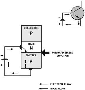
Figure 2-9. - The forward-biased junction in a PNP transistor. PNP REVERSE-BIASED JUNCTION. - In the reverse-biased junction (fig. 2-10), the negative
voltage on the collector and the positive voltage on the base block the majority current carriers from crossing
the junction. However, this same negative collector voltage acts as forward bias for the minority current holes in
the base, which cross the junction and enter the collector. The minority current electrons in the collector also
sense forward bias-the positive base voltage-and move into the base. The holes in the collector are filled by
electrons that flow from the negative terminal of the battery. At the same time the electrons leave the negative
terminal of the battery, other electrons in the base break their covalent bonds and enter the positive terminal of
the battery. Although there is only minority current flow in the reverse-biased junction, it is still very small
because of the limited number of minority current carriers.
2-13

Figure 2-10. - The reverse-biased junction in a PNP transistor. PNP JUNCTION INTERACTION. - The interaction between the forward- and reverse-biased
junctions in a PNP transistor is very similar to that in an NPN transistor, except that in the PNP transistor,
the majority current carriers are holes. In the PNP transistor shown in figure 2-11, the positive voltage on the
emitter repels the holes toward the base. Once in the base, the holes combine with base electrons. But again,
remember that the base region is made very thin to prevent the recombination of holes with electrons. Therefore,
well over 90 percent of the holes that enter the base become attracted to the large negative collector voltage and
pass right through the base. However, for each electron and hole that combine in the base region, another electron
leaves the negative terminal of the base battery (VBB) and enters the base as base current (IB).
At the same time an electron leaves the negative terminal of the battery, another electron leaves the emitter as IE
(creating a new hole) and enters the positive terminal of VBB. Meanwhile, in the collector circuit,
electrons from the collector battery (VCC) enter the collector as Ic and combine with the excess holes
from the base. For each hole that is neutralized in the collector by an electron, another electron leaves the
emitter and starts its way back to the positive terminal of VCC.
2-14
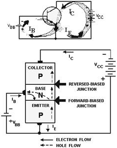
Figure 2-11. - PNP transistor operation. Although current flow in the external circuit of the PNP transistor is opposite in direction to that of
the NPN transistor, the majority carriers always flow from the emitter to the collector. This flow of majority
carriers also results in the formation of two individual current loops within each transistor. One loop is the
base-current path, and the other loop is the collector-current path. The combination of the current in both of
these loops (IB + IC) results in total transistor current (IE). The most
important thing to remember about the two different types of transistors is that the emitter-base voltage of the
PNP transistor has the same controlling effect on collector current as that of the NPN transistor. In simple
terms, increasing the forward- bias voltage of a transistor reduces the emitter-base junction barrier. This action
allows more carriers to reach the collector, causing an increase in current flow from the emitter to the collector
and through the external circuit. Conversely, a decrease in the forward-bias voltage reduces collector current.
Q10. What are the majority current carriers in a PNP transistor? Q11. What is the relationship
between the polarity of the voltage applied to the PNP transistor and that applied to the NPN transistor?
Q12. What is the letter designation for base current? Q13. Name the two current loops in a transistor.
The Basic Transistor Amplifier In the preceding pages we explained the internal workings of the transistor and introduced new terms,
such as emitter, base, and collector. Since you should be familiar by now with all of the new terms
2-15
mentioned earlier and with the internal operation of the transistor, we will move on to the basic transistor
amplifier.
To understand the overall operation of the transistor amplifier, you must only consider the current in
and out of the transistor and through the various components in the circuit. Therefore, from this point on, only
the schematic symbol for the transistor will be used in the illustrations, and rather than thinking about majority
and minority carriers, we will now start thinking in terms of emitter, base, and collector current.
Before going into the basic transistor amplifier, there are two terms you should be familiar with: Amplification
and Amplifier. Amplification is the process of increasing the strength of a Signal. a signal is just a general
term used to refer to any particular current, voltage, or power in a circuit. An amplifier is the
device
that provides amplification (the increase in current, voltage, or power of a signal) without appreciably altering
the original signal. Transistors are frequently used as amplifiers. Some transistor circuits are CURRENT
amplifiers, with a small load resistance; other circuits are designed for Voltage amplification and have a high
load resistance; others amplify Power. Now take a look at the NPN version of the basic transistor
amplifier in figure 2-12 and let's see just how it works. So far in this discussion, a separate battery
has been used to provide the necessary forward-bias voltage. Although a separate battery has been used in the past
for convenience, it is not practical to use a battery for emitter-base bias. For instance, it would take a battery
slightly over .2 volts to properly forward bias a germanium transistor, while a similar silicon transistor would
require a voltage slightly over .6 volts. However, common batteries do not have such voltage values. Also, since
bias voltages are quite critical and must be held within a few tenths of one volt, it is easier to work with bias
currents flowing through resistors of high ohmic values than with batteries. By inserting one or more
resistors in a circuit, different methods of biasing may be achieved and the emitter-base battery eliminated. In
addition to eliminating the battery, some of these biasing methods compensate for slight variations in transistor
characteristics and changes in transistor conduction resulting from temperature irregularities. Notice in figure
2-12 that the emitter-base battery has been eliminated and the bias resistor R B has been inserted between the
collector and the base. Resistor RB provides the necessary forward bias for the emitter-base junction. Current
flows in the emitter-base bias circuit from ground to the emitter, out the base lead, and through R B to V CC.
Since the current in the base circuit is very small (a few hundred microamperes) and the forward resistance of the
transistor is low, only a few tenths of a volt of positive bias will be felt on the base of the transistor.
However, this is enough voltage on the base, along with ground on the emitter and the large positive voltage on
the collector, to properly bias the transistor.
2-16
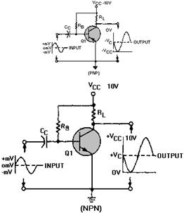
Figure 2-12. - The basic transistor amplifier. With Q1 properly biased, direct current flows continuously, with or without an input signal, throughout
the entire circuit. The direct current flowing through the circuit develops more than just base bias; it also
develops the collector voltage (VC) as it flows through Q1 and RL. Notice the collector
voltage on the output graph. Since it is present in the circuit without an input signal, the output signal starts
at the VC level and either increases or decreases. These dc voltages and currents that exist in the circuit before
the application of a signal are known as QUIESCENT voltages and currents (the quiescent state of the circuit).
Resistor RL, the collector load resistor, is placed in the circuit to keep the full effect of the collector
supply voltage off the collector. This permits the collector voltage (VC) to change with an input
signal, which in turn allows the transistor to amplify voltage. Without RL in the circuit, the voltage on the
collector would always be equal to VCC. The coupling capacitor (CC) is another new
addition to the transistor circuit. It is used to pass the ac input signal and block the dc voltage from the
preceding circuit. This prevents dc in the circuitry on the left of the coupling capacitor from affecting the bias
on Q1. The coupling capacitor also blocks the bias of Q1 from reaching the input signal source. The input
to the amplifier is a sine wave that varies a few millivolts above and below zero. It is introduced into the
circuit by the coupling capacitor and is applied between the base and emitter. As the input signal goes positive,
the voltage across the emitter-base junction becomes more positive. This in effect increases forward bias, which
causes base current to increase at the same rate as that of the input sine wave. Emitter and collector currents
also increase but much more than the base current. With an increase in collector current, more voltage is
developed across RL. Since the voltage across RL
and the voltage across Q1 (collector to emitter) must add up to VCC, an increase in voltage across RL
results in an equal decrease in
2-17
voltage across Q1. Therefore, the output voltage from the amplifier, taken at the collector of Q1 with
respect to the emitter, is a negative alternation of voltage that is larger than the input, but has the same sine
wave characteristics. During the negative alternation of the input, the input signal opposes the forward
bias. This action decreases base current, which results in a decrease in both emitter and collector currents. The
decrease in current through RL decreases its voltage drop and causes the voltage across the transistor
to rise along with the output voltage. Therefore, the output for the negative alternation of the input is a
positive alternation of voltage that is larger than the input but has the same sine wave characteristics.
By examining both input and output signals for one complete alternation of the input, we can see that the output
of the amplifier is an exact reproduction of the input except for the reversal in polarity and the increased
amplitude (a few millivolts as compared to a few volts). The PNP version of this amplifier is shown in
the upper part of the figure. The primary difference between the NPN and PNP amplifier is the polarity of the
source voltage. With a negative VCC, the PNP base voltage is slightly negative with respect to ground,
which provides the necessary forward bias condition between the emitter and base. When the PNP input
signal goes positive, it opposes the forward bias of the transistor. This action cancels some of the negative
voltage across the emitter-base junction, which reduces the current through the transistor. Therefore, the voltage
across the load resistor decreases, and the voltage across the transistor increases. Since VCC is
negative, the voltage on the collector (VC) goes in a negative direction (as shown on the output graph)
toward -VCC (for example, from -5 volts to -7 volts). Thus, the output is a negative alternation of
voltage that varies at the same rate as the sine wave input, but it is opposite in polarity and has a much larger
amplitude. During the negative alternation of the input signal, the transistor current increases because
the input voltage aids the forward bias. Therefore, the voltage across RL increases, and consequently, the voltage
across the transistor decreases or goes in a positive direction (for example: from -5 volts to -3 volts). This
action results in a positive output voltage, which has the same characteristics as the input except that it has
been amplified and the polarity is reversed. In summary, the input signals in the preceding circuits were
amplified because the small change in base current caused a large change in collector current. And, by placing
resistor RL in series with the collector, voltage amplification was achieved.
Q14. What is the name of the device that provides an increase in current, voltage, or power of a signal
without appreciably altering the original signal? Q15. Besides eliminating the emitter-base battery,
what other advantages can different biasing methods offer? Q16. In the basic transistor amplifier
discussed earlier, what is the relationship between the polarity of the input and output signals? Q17.
What is the primary difference between the NPN and PNP amplifiers?
TYPES of BIAS One of the basic problems with transistor amplifiers is establishing and
maintaining the proper values of quiescent current and voltage in the circuit. This is accomplished by selecting
the proper circuit-biasing conditions and ensuring these conditions are maintained despite variations in ambient
(surrounding)
2-18
temperature, which cause changes in amplification and even distortion (an unwanted change in a
signal). Thus a need arises for a method to properly bias the transistor amplifier and at the same time stabilize
its dc operating point (the no signal values of collector voltage and collector current). As mentioned earlier,
various biasing methods can be used to accomplish both of these functions. Although there are numerous biasing
methods, only three basic types will be considered. Base-Current Bias (Fixed Bias)
The first biasing method, called Base CURRENT BIAS or sometimes FIXED BIAS, was used in figure 2-12. As you
recall, it consisted basically of a resistor (RB) connected between the collector supply voltage and
the base. Unfortunately, this simple arrangement is quite thermally unstable. If the temperature of the transistor
rises for any reason (due to a rise in ambient temperature or due to current flow through it), collector current
will increase. This increase in current also causes the dc operating point, sometimes called the quiescent or
static point, to move away from its desired position (level). This reaction to temperature is undesirable because
it affects amplifier gain (the number of times of amplification) and could result in distortion, as you will see
later in this discussion.
Self-Bias A better method of biasing is obtained by inserting the bias resistor directly between
the base and collector, as shown in figure 2-13. By tying the collector to the base in this manner, feedback
voltage can be fed from the collector to the base to develop forward bias. This arrangement is called SELF-BIAS.
Now, if an increase of temperature causes an increase in collector current, the collector voltage (VC)
will fall because of the increase of voltage produced across the load resistor (RL). This drop in VC
will be fed back to the base and will result in a decrease in the base current. The decrease in base current will
oppose the original increase in collector current and tend to stabilize it. The exact opposite effect is produced
when the collector current decreases.
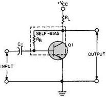
Figure 2-13. - a basic transistor amplifier with self-bias. Self-bias has two small drawbacks: (1) It is only partially effective and, therefore, is only used where
moderate changes in ambient temperature are expected; (2) it reduces amplification since the signal on the
collector also affects the base voltage. This is because the collector and base signals for this particular
amplifier configuration are 180 degrees out of phase (opposite in polarity) and the part of the collector signal
that is fed back to the base cancels some of the input signal. This process of returning a part of the output back
to its input is known as DEGENERATION or Negative Feedback. Sometimes degeneration is
2-19
desired to prevent amplitude distortion (an output signal that fails to follow the input exactly) and
self-bias may be used for this purpose. Combination Bias A combination of fixed
and self-bias can be used to improve stability and at the same time overcome some of the disadvantages of the
other two biasing methods. One of the most widely used combination-bias systems is the voltage-divider type shown
in figure 2-14. Fixed bias is provided in this circuit by the voltage- divider network consisting of R1, R2, and
the collector supply voltage (VCC). The dc current flowing through the voltage-divider network biases
the base positive with respect to the emitter. Resistor R3, which is connected in series with the emitter,
provides the emitter with self-bias. Should IE increase, the voltage drop across R3 would also
increase, reducing VC. This reaction to an increase in IE by R3 is another form of
degeneration, which results in less output from the amplifier. However, to provide long-term or dc thermal
stability, and at the same time, allow minimal ac signal degeneration, the bypass capacitor (Cbp) is
placed across R3. If Cbp is large enough, rapid signal variations will not change its charge materially
and no degeneration of the signal will occur.

Figure 2-14. - a basic transistor amplifier with combination bias. In summary, the fixed-bias resistors, R1 and R2, tend to keep the base bias constant while the emitter
bias changes with emitter conduction. This action greatly improves thermal stability and at the same time
maintains the correct operating point for the transistor. Q18. Which biasing method is the most
unstable?
Q19. What type of bias is used where only moderate changes in ambient temperature are expected?
Q20. When is degeneration tolerable in an amplifier? Q21. What is the most widely used
combination-bias system?
2-20
| - |
Matter, Energy,
and Direct Current |
| - |
Alternating Current and Transformers |
| - |
Circuit Protection, Control, and Measurement |
| - |
Electrical Conductors, Wiring Techniques,
and Schematic Reading |
| - |
Generators and Motors |
| - |
Electronic Emission, Tubes, and Power Supplies |
| - |
Solid-State Devices and Power Supplies |
| - |
Amplifiers |
| - |
Wave-Generation and Wave-Shaping Circuits |
| - |
Wave Propagation, Transmission Lines, and
Antennas |
| - |
Microwave Principles |
| - |
Modulation Principles |
| - |
Introduction to Number Systems and Logic Circuits |
| - |
- Introduction to Microelectronics |
| - |
Principles of Synchros, Servos, and Gyros |
| - |
Introduction to Test Equipment |
| - |
Radio-Frequency Communications Principles |
| - |
Radar Principles |
| - |
The Technician's Handbook, Master Glossary |
| - |
Test Methods and Practices |
| - |
Introduction to Digital Computers |
| - |
Magnetic Recording |
| - |
Introduction to Fiber Optics |
| Note: Navy Electricity and Electronics Training
Series (NEETS) content is U.S. Navy property in the public domain. |
|