Module 7 - Introduction to Solid-State Devices and Power Supplies
Pages i ,
1-1,
1-11,
1-21,
1-31,
1-41,
2-1,
2-11,
2-21,
2-31,
2-41,
2-51,
3-1,
3-11,
3-21,
3-31,
3-41,
3-51,
4-1 to 4-10,
4-11,
4-21,
4-31,
4-41,
4-51, Index
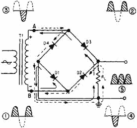
Figure 4-8. - Bridge rectifier. One complete cycle of operation will be discussed to help you understand how this circuit works. We have
discussed transformers in previous modules in the NEETS series and will not go into their characteristics at this
time. Let us assume the transformer is working properly and there is a positive potential at point a and a
negative potential at point B. The positive potential at point a will forward bias D3 and reverse bias D4. The
negative potential at point B will forward bias D1 and reverse bias D2. At this time D3 and D1 are forward biased
and will allow current flow to pass through them; D4 and D2 are reverse biased and will block current flow. The
path for current flow is from point B through D1, up through RL, through D3, through the secondary of
the transformer back to point B. This path is indicated by the solid arrows. Waveforms (1) and (2) can be observed
across D1 and D3.
One-half cycle later the polarity across the secondary of the transformer reverses, forward biasing D2 and D4 and
reverse biasing D1 and D3. Current flow will now be from point a through D4, up through RL, through D2,
through the secondary of T1, and back to point A. This path is indicated by the broken arrows. Waveforms (3) and
(4) can be observed across D2 and D4. You should have noted that the current flow through RL is always
in the same direction. In flowing through RL this current develops a voltage corresponding to that
shown in waveform (5). Since current flows through the load (RL) during both half cycles of the applied
voltage, this bridge rectifier is a full-wave rectifier. One advantage of a bridge rectifier over a
conventional full-wave rectifier is that with a given transformer the bridge rectifier produces a voltage output
that is nearly twice that of the conventional full- wave circuit. This may be shown by assigning values to some of
the components shown in views a and B of figure 4-9. Assume that the same transformer is used in both circuits.
The peak voltage developed between points X and Y is 1000 volts in both circuits. In the conventional full-wave
circuit shown in view A, the peak voltage from the center tap to either X or Y is 500 volts. Since only one diode
can conduct at any instant, the maximum voltage that can be rectified at any instant is 500 volts. Therefore, the
maximum voltage that appears across the load resistor is nearly - but never exceeds - 500 volts, as a result of
the small voltage drop across the diode. In the bridge rectifier shown in view B, the maximum voltage that can be
rectified is the full secondary voltage, which is 1000 volts. Therefore, the peak output
4-11
voltage across the load resistor is nearly 1000 volts. With both circuits using the same transformer,
the bridge rectifier circuit produces a higher output voltage than the conventional full-wave rectifier circuit.
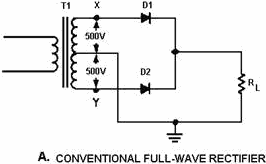
Figure 4-9A. - Comparison of a conventional and bridge full-wave rectifier. CONVENTIONAL FULL-WAVE
RECTIFIER
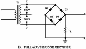
Figure 4-9B. - Comparison of a conventional and bridge full-wave rectifier. FULL-WAVE BRIDGE
RECTIFIER Q11. What is the main disadvantage of a conventional full-wave rectifier?
Q12. What main advantage does a bridge rectifier have over a conventional full-wave rectifier?
FILTERS While the output of a rectifier is a pulsating dc, most electronic circuits
require a substantially pure dc for proper operation. This type of output is provided by single or multisection
filter circuits placed between the output of the rectifier and the load. There are four basic types of
filter circuits:
· Simple capacitor filter
· LC choke-input filter
4-12
· LC capacitor-input filter (pi-type)
· RC capacitor-input filter (pi-type) The
function of each of these filters will be covered in detail in this chapter.
Filtering is accomplished by the use of capacitors, inductors, and/or resistors in various combinations. Inductors
are used as series impedances to oppose the flow of alternating (pulsating dc) current. Capacitors are used as
shunt elements to bypass the alternating components of the signal around the load (to ground). Resistors are used
in place of inductors in low current applications. Let's briefly review the properties of a capacitor.
First, a capacitor opposes any change in voltage. The opposition to a change in current is called capacitive
reactance (XC) and is measured in ohms. The capacitive reactance is determined by the frequency (f) of
the applied voltage and the capacitance (C) of the capacitor.
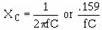
From the formula, you can see that if frequency or capacitance is increased, the XC
decreases. Since filter capacitors are placed in parallel with the load, a low XC will provide better
filtering than a high XC. For this to be accomplished, a better shunting effect of the ac around the
load is provided, as shown in figure 4-10. To obtain a steady dc output, the capacitor must charge almost
instantaneously to the value of applied voltage. Once charged, the capacitor must retain the charge as long as
possible. The capacitor must have a short charge time constant (view A). This can be accomplished by keeping the
internal resistance of the power supply as small as possible (fast charge time) and the resistance of the load as
large as possible (for a slow discharge time as illustrated in view B).
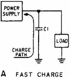
Figure 4-10A. - Capacitor filter. FAST CHARGE 4-13
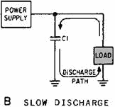
Figure 4-10B. - Capacitor filter. SLow DIsCHARGE From your earlier studies in basic electricity, you may remember that one time constant is defined as
the time it takes a capacitor to charge to 63.2 percent of the applied voltage or to discharge to 36.8 percent of
its total charge. This action can be expressed by the following equation:
t = RC Where: R represents the resistance of the charge or discharge path And: C represents the
capacitance of the capacitor. You should also recall that a capacitor is considered fully charged after
five RC time constants. Refer to figure 4-11. You can see that a steady dc output voltage is obtained when the
capacitor charges rapidly and discharges as slowly as possible.
4-14
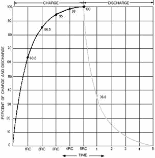
Figure 4-11. - RC time constant. In filter circuits the capacitor is the common element to both the charge and the discharge paths.
Therefore, to obtain the longest possible discharge time, you want the capacitor to be as large as possible.
Another way to look at it is: The capacitor acts as a short circuit around the load (as far as the ac component is
concerned), and since

the larger the value of the capacitor (C), the smaller the opposition (XC) or reactance to
ac. Now let's look at inductors and their application in filter circuits. Remember, an INDUCTOR OPPOSES ANY CHANGE
IN CURRENT. In case you have forgotten, a change in current through an inductor produces a changing
electromagnetic field. The changing field, in turn, cuts the windings of the wire in the inductor and thereby
produces a counter electromotive force (CEMF). It is the CEMF that opposes the change in circuit current.
Opposition to a change in current at a given frequency is called inductive reactance (XL) and is
measured in ohms. The inductive reactance (XL) of an inductor is determined by the applied frequency
and the inductance of the inductor. Mathematically,
XL = 2πfL If frequency or inductance is increased, the XL increases. Since inductors are placed in series with
the load (as shown in figure 4-12), the larger the XL, the larger the ac voltage developed across the load.
4-15
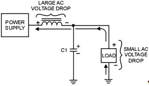
Figure 4-12. - Voltage drops in an inductive filter. Now refer to figure 4-13. When the current starts to flow through the coil, an expanding magnetic field
builds up around the inductor. This magnetic field around the coil develops the CEMF that opposes the change in
current. When the rectifier current decreases, as shown in figure 4-14, the magnetic field collapses and again
cuts the turns (windings) of wire, thus inducing current into the coil. This additional current merges with the
rectifier current and attempts to keep it at its original level.
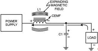
Figure 4-13. - Inductive filter (expanding field). 4-16
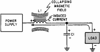
Figure 4-14. - Inductive filter (collapsing field). Now that you have read how the components in a filter circuit react to current flow from the rectifier,
the different types of filter circuits in use today will be discussed. Q13. If you increase the value of
the capacitor, will the XC increase or decrease? Why? The Capacitor Filter
The simple capacitor filter is the most basic type of power supply filter. The application of the simple
capacitor filter is very limited. It is sometimes used on extremely high-voltage, low-current power supplies for
cathode-ray and similar electron tubes, which require very little load current from the supply. The capacitor
filter is also used where the power-supply ripple frequency is not critical; this frequency can be relatively
high. The capacitor (C1) shown in figure 4-15 is a simple filter connected across the output of the rectifier in
parallel with the load.

Figure 4-15. - Full-wave rectifier with a capacitor filter. When this filter is used, the RC charge time of the filter capacitor (C1) must be short and the RC
discharge time must be long to eliminate ripple action. In other words, the capacitor must charge up fast,
preferably with no discharge at all. Better filtering also results when the input frequency is high; therefore,
the full-wave rectifier output is easier to filter than that of the half-wave rectifier because of its higher
frequency.
For you to have a better understanding of the effect that filtering has on Eavg, a comparison of a
rectifier circuit with a filter and one without a filter is illustrated in views a and B of figure 4-16. The
4-17
output waveforms in figure 4-16 represent the unfiltered and filtered outputs of the half-wave
rectifier circuit. Current pulses flow through the load resistance (RL) each time a diode conducts. The
dashed line indicates the average value of output voltage. For the half-wave rectifier, Eavg is less
than half (or approximately 0.318) of the peak output voltage. This value is still much less than that of the
applied voltage. With no capacitor connected across the output of the rectifier circuit, the waveform in view a
has a large pulsating component (ripple) compared with the average or dc component. When a capacitor is connected
across the output (view B), the average value of output voltage (Eavg) is increased due to the
filtering action of capacitor C1.
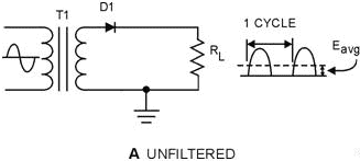
Figure 4-16A. - Half-wave rectifier with and without filtering. UNFILTERED
Figure 4-16B. - Half-wave rectifier with and without filtering. FILTERED The value of the capacitor is fairly large (several microfarads), thus it presents a relatively low
reactance to the pulsating current and it stores a substantial charge. The rate of charge for the
capacitor is limited only by the resistance of the conducting diode which is relatively low. Therefore, the RC
charge time of the circuit is relatively short. As a result, when the pulsating voltage is first applied to the
circuit, the capacitor charges rapidly and almost reaches the peak value of the rectified voltage within the first
few cycles. The capacitor attempts to charge to the peak value of the rectified voltage anytime a diode is
conducting, and tends to retain its charge when the
4-18
rectifier output falls to zero. (The capacitor cannot discharge immediately.) The capacitor slowly
discharges through the load resistance (RL) during the time the rectifier is nonconducting. The
rate of discharge of the capacitor is determined by the value of capacitance and the value of the load resistance.
If the capacitance and load-resistance values are large, the RC discharge time for the circuit is relatively long.
a comparison of the waveforms shown in figure 4-16 (view a and view B) illustrates that the addition of C1 to the
circuit results in an increase in the average of the output voltage (Eavg) and a reduction in the
amplitude of the ripple component (Er) which is normally present across the load resistance.
Now, let's consider a complete cycle of operation using a half-wave rectifier, a capacitive filter (C1), and a
load resistor (RL). As shown in view a of figure 4-17, the capacitive filter (C1) is assumed to be large enough to
ensure a small reactance to the pulsating rectified current. The resistance of RL is assumed to be much greater
than the reactance of C1 at the input frequency. When the circuit is energized, the diode conducts on the positive
half cycle and current flows through the circuit, allowing C1 to charge. C1 will charge to approximately the peak
value of the input voltage. (The charge is less than the peak value because of the voltage drop across the diode
(D1)). In view a of the figure, the charge on C1 is indicated by the heavy solid line on the waveform. As
illustrated in view B, the diode cannot conduct on the negative half cycle because the anode of D1 is negative
with respect to the cathode. During this interval, C1 discharges through the load resistor (RL). The
discharge of C1 produces the downward slope as indicated by the solid line on the waveform in view B. In contrast
to the abrupt fall of the applied ac voltage from peak value to zero, the voltage across C1 (and thus across RL)
during the discharge period gradually decreases until the time of the next half cycle of rectifier operation. Keep
in mind that for good filtering, the filter capacitor should charge up as fast as possible and discharge as little
as possible.
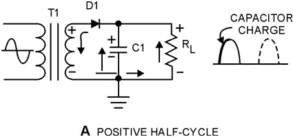
Figure 4-17A. - Capacitor filter circuit (positive and negative half cycles). Positive Half-Cycle 4-19
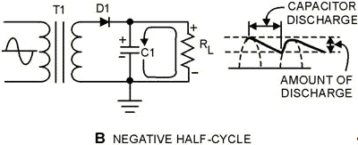
Figure 4-17B. - Capacitor filter circuit (positive and negative half cycles). Negative Half-Cycle Since practical values of C1 and RL ensure a more or less gradual decrease of the discharge voltage, a
substantial charge remains on the capacitor at the time of the next half cycle of operation. As a result, no
current can flow through the diode until the rising ac input voltage at the anode of the diode exceeds the voltage
on the charge remaining on C1. The charge on C1 is the cathode potential of the diode. When the potential on the
anode exceeds the potential on the cathode (the charge on C1), the diode again conducts, and C1 begins to charge
to approximately the peak value of the applied voltage. After the capacitor has charged to its peak value,
the diode will cut off and the capacitor will start to discharge. Since the fall of the ac input voltage on the
anode is considerably more rapid than the decrease on the capacitor voltage, the cathode quickly become more
positive than the anode, and the diode ceases to conduct. Operation of the simple capacitor filter using a
full-wave rectifier is basically the same as that discussed for the half-wave rectifier. Referring to figure 4-18,
you should notice that because one of the diodes is always conducting on. either alternation, the filter capacitor
charges and discharges during each half cycle. (Note that each diode conducts only for that portion of time when
the peak secondary voltage is greater than the charge across the capacitor.)
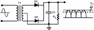
Figure 4-18. - Full-wave rectifier (with capacitor filter). Another thing to keep in mind is that the ripple component (E) of the output voltage is an ac voltage
and the average output voltage (Eavg) is the dc component of the output. Since the filter capacitor
offers a relatively low impedance to ac, the majority of the ac component flows through the filter capacitor. The
ac component is therefore bypassed (shunted) around the load resistance, and the entire dc component (or
4-20
| - |
Matter, Energy,
and Direct Current |
| - |
Alternating Current and Transformers |
| - |
Circuit Protection, Control, and Measurement |
| - |
Electrical Conductors, Wiring Techniques,
and Schematic Reading |
| - |
Generators and Motors |
| - |
Electronic Emission, Tubes, and Power Supplies |
| - |
Solid-State Devices and Power Supplies |
| - |
Amplifiers |
| - |
Wave-Generation and Wave-Shaping Circuits |
| - |
Wave Propagation, Transmission Lines, and
Antennas |
| - |
Microwave Principles |
| - |
Modulation Principles |
| - |
Introduction to Number Systems and Logic Circuits |
| - |
- Introduction to Microelectronics |
| - |
Principles of Synchros, Servos, and Gyros |
| - |
Introduction to Test Equipment |
| - |
Radio-Frequency Communications Principles |
| - |
Radar Principles |
| - |
The Technician's Handbook, Master Glossary |
| - |
Test Methods and Practices |
| - |
Introduction to Digital Computers |
| - |
Magnetic Recording |
| - |
Introduction to Fiber Optics |
| Note: Navy Electricity and Electronics Training
Series (NEETS) content is U.S. Navy property in the public domain. |
|