Module 7 - Introduction to Solid-State Devices and Power Supplies
Pages i ,
1-1,
1-11,
1-21,
1-31,
1-41,
2-1,
2-11,
2-21,
2-31,
2-41,
2-51,
3-1,
3-11,
3-21,
3-31,
3-41,
3-51,
4-1 to 4-10,
4-11,
4-21,
4-31,
4-41,
4-51, Index
forward bias of Q1 changes
to 0.6 volt. Because this bias voltage is less than the normal 0.7 volt, the resistance of Q1 increases, thereby
increasing the voltage drop across the transistor to 5.8 volts. This voltage drop restores the output voltage to
14.3 volts. The entire cycle takes only a fraction of a second and, therefore, the change is not visible on an
oscilloscope or readily measurable with other standard test equipment.
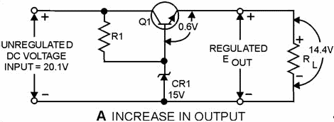
Figure 4-36A. - Series voltage regulator. INCREASE IN Output View B is a schematic diagram for the same series voltage regulator with one significant difference. The
output voltage is shown as 14.2 volts instead of the desired 14.3 volts. In this case, the load has increased
causing a lowered voltage drop across R L to 14.2 volts. When the output decreases, the forward bias of Q1
increases to 0.8 volt because Zener diode CR1 maintains the base voltage of Q1 at 15 volts. This 0.8 volt is the
difference between the Zener reference voltage of 15 volts and the momentary output voltage. (15 V - 14.2 V = 0.8
V). At this point, the larger forward bias on Q1 causes the resistance of Q1 to decrease, thereby causing the
voltage drop across Q1 to return to 5.7 volts. This then causes the output voltage to return to 14.3 volts.

Figure 4-36B. - Series voltage regulator. DECREASE IN Output 4-41
The schematic shown in figure 4-37 is that of a shunt voltage regulator. Notice that Q1 is in parallel
with the load. Components of this circuit are identical with those of the series voltage regulator except for the
addition of fixed resistor RS. As you study the schematic, you will see that this resistor is connected
in series with the output load resistance. The current limiting resistor (R1) and Zener diode (CR1) provide a
constant reference voltage for the base-collector junction of Q1. Notice that the bias of Q1 is determined by the
voltage drop across RS and R1. As you should know, the amount of forward bias across a transistor
affects its total resistance. In this case, the voltage drop across RS is the key to the total circuit
operation.

Figure 4-37. - Shunt voltage regulator. Figure 4-38 is the schematic for a typical shunt-type regulator. Notice that the schematic is identical
to the schematic shown in figure 4-37 except that voltages are shown to help you understand the functions of the
various components. In the circuit shown, the voltage drop across the Zener diode (CR1) remains constant at 5.6
volts. This means that with a 20-volt input voltage, the voltage drop across R1 is 14.4 volts. With a base-emitter
voltage of 0.7 volt, the output voltage is equal to the sum of the voltages across CR1 and the voltage at the
base-emitter junction of Q1. In this example, with an output voltage of 6.3 volts and a 20-volt input voltage, the
voltage drop across RS equals 13.7 volts. Study the schematic to understand fully how these voltages are
developed. Pay close attention to the voltages shown.
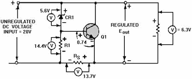
Figure 4-38. - Shunt voltage regulator (with voltages). 4-42
Now, refer to view a of figure 4-39. This figure shows the schematic diagram of the same shunt voltage
regulator as that shown in figure 4-38 with an increased input voltage of 20.1 volts. This increases the forward
bias on Q1 to 0.8 volt. Recall that the voltage drop across CR1 remains constant at 5.6 volts. Since the output
voltage is composed of the Zener voltage and the base-emitter voltage, the output voltage momentarily increases to
6.4 volts. At this time, the increase in the forward bias of Q1 lowers the resistance of the transistor allowing
more current to flow through it. Since this current must also pass through RS, there is also an
increase in the voltage drop across this resistor. The voltage drop across RS is now 13.8 volts and
therefore the output voltage is reduced to 6.3 volts. Remember, this change takes place in a fraction of a second.

Figure 4-39A. - Shunt voltage regulator. INCREASE IN Output Voltage Study the schematic shown in view B. Although this schematic is identical to the other shunt voltage
schematics previously illustrated and discussed, the output voltage is different. The load current has increased
causing a momentary drop in voltage output to 6.2 volts. Recall that the circuit was designed to ensure a constant
output voltage of 6.3 volts. Since the output voltage is less than that required, changes occur in the regulator
to restore the output to 6.3 volts. Because of the 0.1 volt drop in the output voltage, the forward bias of Q1 is
now 0.6 volt. This decrease in the forward bias increases the resistance of the transistor, thereby reducing the
current flow through Q1 by the same amount that the load current increased. The current flow through RS
returns to its normal value and restores the output voltage to 6.3 volts.
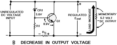
Figure 4-39B. - Shunt voltage regulator. DECREASE IN Output Voltage 4-43
Q33. In figure 4-37, the voltage drop across RS and R1 determines the amount of base-emitter for Q1.
Q34. In figure 4-39, view A, when there is an increase in the input voltage, the forward bias of Q1
increases/decreases (which one). Q35. In view B of figure 4-39, when the load current increases and the
output voltage momentarily drops, the resistance of Q1 increase/decreases (which one) to compensate.
Current Regulators You should now know how voltage regulators work to provide constant output
voltages. In some circuits it may be necessary to regulate the current output. The circuitry which provides a
constant current output is called a constant current regulator or just CURRENT REGULATOR. The schematic shown in
figure 4-40 is a simplified schematic for a current regulator. The variable resistor shown on the schematic is used to illustrate the concept of current regulation. You should know from your study of voltage regulators that a
variable resistor does not respond quickly enough to compensate for the changes. Notice that an ammeter has been
included in this circuit to indicate that the circuit shown is that of a current regulator. When the circuit
functions properly, the current reading of the ammeter remains constant. In this case the variable resistor (RV)
compensates for changes in the load or dc input voltage. Adequate current regulation results in the loss of
voltage regulation. Studying the schematic shown, you should recall that any increase in load resistance causes a
drop in current. To maintain a constant current flow, the resistance of RV must be reduced whenever the
load resistance increases. This causes the total resistance to remain constant. An increase in the input voltage
must be compensated for by an increase in the resistance of RV, thereby maintaining a constant current
flow. The operation of a current regulator is similar to that of a voltage regulator. The basic difference is that
one regulates current and the other regulates voltage.

Figure 4-40. - Current regulator (simplified). Since use of a variable resistor is not a practical way to control current fluctuation or variation, a
transistor and a Zener diode, together with necessary resistors, are used. Recall that the Zener diode provides a
constant reference voltage. The schematic shown in figure 4-41 is that of a current regulator circuit. Except for
the addition of R1, the circuit shown in the figure is similar to that of a series voltage regulator. The resistor
is connected in series with the load and senses any current changes in the load. Notice the voltage drop across R1
and the negative voltage polarity applied to the emitter of Q1. The
4-44
voltage polarity is a result of current flowing through R1, and this negative voltage opposes the
forward bias for Q1. However, since the regulated voltage across CR1 has an opposite polarity, the actual bias of
the transistor is the difference between the two voltages. You should see that the purpose of R2 is to function as
a current-limiting resistor for the Zener diode.
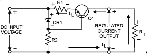
Figure 4-41. - Current regulator. The purpose of a current regulator is to provide a constant current regardless of changes in the input
voltage or load current. The schematic shown in figure 4-42 is that of a circuit designed to provide a constant
current of 400 milliamperes. Voltmeters are shown in the schematic to emphasize the voltage drops across specific
components. These voltages will help you understand how the current regulator operates. The voltage drop across
the base-emitter junction of Q1 is 0.6 volt. This voltage is the difference between the Zener voltage and the
voltage drop across R1. The 0.6-volt forward bias of Q1 permits proper operation of the transistor. The output
voltage across RL
is 6 volts as shown by the voltmeter. With a regulated current output of 400 milliamperes, the transistor
resistance (RQ1) is 9 ohms. This can be proved by using Ohm's law and the values shown on the
schematic. In this case, current (I) is equal to the voltage drop (E) divided by the resistance (R). Therefore: 12
volts divided by 30 ohms equals 0.4 ampere, or 400 milliamperes.
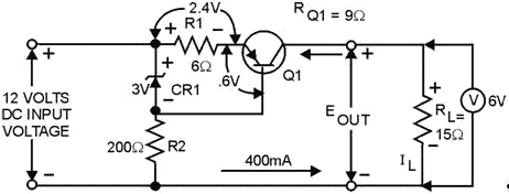
Figure 4-42. - Current regulator (with circuit values). 4-45
Since you are familiar with the basic current regulating circuitry, let's examine in detail how the
various components work to maintain the constant 400-milliampere output. Refer to the schematic shown in figure
4-43. Remember a decrease in load resistance causes a corresponding increase in current flow. In the example
shown, the load resistance RL has dropped from 15 ohms to 10 ohms. This results in a larger voltage
drop across R1 because of the increased current flow. The voltage drop has increased from 2.4 volts to 2.5 volts.
Of course, the voltage drop across CR1 remains constant at 9 volts due to its regulating ability. Because of the
increased voltage drop across R1, the forward bias on Q1 is now 0.5 volt. Since the forward bias of Q1 has
decreased, the resistance of the transistor increases from 9 ohms to 14 ohms. Notice that the 5 ohm increase in
resistance across the transistor corresponds to the 5 ohm decrease in the load resistance. Thus, the total
resistance around the outside loop of the circuit remains constant. Since the circuit is a current regulator, you
know that output voltages will vary as the regulator maintains a constant current output. In the figure, the
voltage output is reduced to 4 volts, which is computed by multiplying current (I) times resistance (R) (400 mA x
10 ohms = 4 volts).
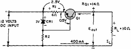
Figure 4-43. - Current regulator (with a decrease in RL). Q36. In figure 4-40, when there is an increase in the load resistance (RL), the
resistance of RV increases/decreases (which one) to compensate for the change. Q37. In
figure 4-43 any decrease in the base-emitter forward bias across Q1 results in an increase/a decrease (which one)
in the resistance of the transistor. Voltage MULTIPLIERS You may already know how
a transformer functions to increase or decrease voltages. You may also have learned that a transformer secondary
may provide one or several ac voltage outputs which may be greater or less than the input voltage. When voltages
are stepped up, current is decreased; when voltages are stepped down, current is increased. Another method
for increasing voltages is known as voltage multiplication. Voltage MULTIPLIERS are used primarily to develop high
voltages where low current is required. The most common application of the high voltage outputs of voltage
multipliers is the anode of cathode-ray tubes (CRT), which are used for radar scope presentations, oscilloscope
presentations, or TV picture tubes. The dc output of the voltage multiplier ranges from 1000 volts to 30,000
volts. The actual voltage depends upon the size of the CRT and its equipment application.
4-46
Voltage multipliers may also be used as primary power supplies where a 177 volt-ac input is rectified
to pulsating dc. This dc output voltage may be increased (through use of a voltage multiplier) to as much as 1000
volts dc. This voltage is generally used as the plate or screen grid voltage for electron tubes. If you
have studied transformers, you may have learned that when voltage is stepped up, the output current decreases.
This is also true of voltage multipliers. Although the measured output voltage of a voltage multiplier may be
several times greater than the input voltage, once a load is connected the value of the output voltage decreases.
Also any small fluctuation of load impedance causes a large fluctuation in the output voltage of the multiplier.
For this reason, voltage multipliers are used only in special applications where the load is constant and has a
high impedance or where input voltage stability is not critical. Voltage multipliers may be classified as
voltage doublers, triplers, or quadruplers. The classification depends on the ratio of the output voltage to the
input voltage. For example, a voltage multiplier that increases the peak input voltage twice is called a voltage
doubler. Voltage multipliers increase voltages through the use of series-aiding voltage sources. This can be
compared to the connection of dry cells (batteries) in series. The figures used in the explanation of
voltage multipliers show a transformer input, even though for some applications a transformer is not necessary.
The input could be directly from the power source or line voltage. This, of course, does not isolate the equipment
from the line and creates a potentially hazardous condition. Most military equipments use transformers to minimize
this hazard. Figure 4-44 shows the schematic for a half-wave voltage doubler. Notice the similarities
between this schematic and those of half-wave voltage rectifiers. In fact, the doubler shown is made up of two
half-wave voltage rectifiers. C1 and CR1 make up one half-wave rectifier, and C2 and CR2 make up the other. The
schematic of the first half-wave rectifier is indicated by the dark lines in view a of figure 4-45. The dotted
lines and associated components represent the other half-wave rectifier and load resistor.

Figure 4-44. - Half-wave voltage doubler. 4-47

Figure 4-45A. - Rectifier action of CR1 and CR2. Positive ALTERNATION Notice that C1 and CR1 work exactly like a half-wave rectifier. During the positive alternation of the
input cycle (view A), the polarity across the secondary winding of the transformer is as shown. Note that the top
of the secondary is negative. At this time CR1 is forward biased (cathode negative in respect to the anode). This
forward bias causes CR1 to function like a closed switch and allows current to follow the path indicated by the
arrows. At this time, C1 charges to the peak value of the input voltage, or 200 volts, with the polarity shown.
During the period when the input cycle is negative, as shown in view B, the polarity across the secondary of the
transformer is reversed. Note specifically that the top of the secondary winding is now positive. This condition
now forward biases CR2 and reverse biases CR1. a series circuit now exists consisting of C1, CR2, C2, and the
secondary of the transformer. The current flow is indicated by the arrows. The secondary voltage of the
transformer now aids the voltage on C1. This results in a pulsating dc voltage of 400 volts, as shown by the
waveform. The effect of series aiding is comparable to the connection of two 200-volt batteries in series. As
shown in figure 4-46, C2 charges to the sum of these voltages, or 400 volts.

Figure 4-45B. - Rectifier action of CR1 and CR2. Negative ALTERNATION 4-48
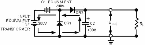
Figure 4-46. - Series-aiding sources. The schematic shown in figure 4-47 is an illustration of a half-wave voltage tripler. When you compare
figures 4-46 and 4-47, you should see that the circuitry is identical except for the additional parts, components,
and circuitry shown by the dotted lines. (CR3, C3, and R2 make up the additional circuitry.) By themselves, CR3,
C3, and R2 make up a half-wave rectifier. Of course, if you remove the added circuitry, you will once again have a
half-wave voltage doubler.
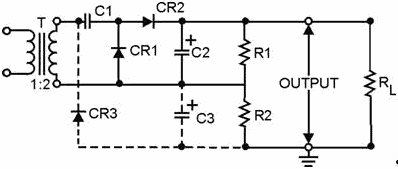
Figure 4-47. - Half-wave voltage tripler. View a of figure 4-48 shows the schematic for the voltage tripler. Notice that CR3 is forward biased and
functions like a closed switch. This allows C3 to charge to a peak voltage of 200 volts at the same time C1 is
also charging to 200 volts.
4-49
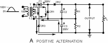
Figure 4-48A. - Voltage tripler. Positive ALTERNATION The other half of the input cycle is shown in view B. C2 is charged to twice the input voltage, or 400
volts, as a result of the voltage-doubling action of the transformer and C1. At this time, C2 and C3 are used as
series-aiding devices, and the output voltage increases to the sum of their respective voltages, or 600 volts. R1
and R2 are proportional according to the voltages across C2 and C3. In this case, there is a 2 to 1 ratio.
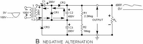
Figure 4-48B. - Voltage tripler. Negative ALTERNATION The circuit shown in figure 4-49 is that of a full-wave voltage doubler. The main advantage of a
full-wave doubler over a half-wave doubler is better voltage regulation, as a result of reduction in the output
ripple amplitude and an increase in the ripple frequency. The circuit is, in fact, two half-wave rectifiers. These
rectifiers function as series-aiding devices except in a slightly different way. During the alternation when the
secondary of the transformer is positive at the top, C1 charges to 200 volts through CR1. Then, when the
transformer secondary is negative at the top, C2 charges to 200 volts through CR2. R1 and R2 are equal value,
balancing resistors that stabilize the charges of the two capacitors. Resistive load RL is connected
across C1 and C2 so that R L receives the total charge of both capacitors. The output voltage is +400 volts when
measured at the top of R L, or point "A" with respect to point "B." If the output is measured at the bottom of RL,
it is -400 volts. Either way, the output is twice the peak value of the ac secondary voltage. As you can imagine,
the possibilities for voltage multiplication are extensive.
4-50
| - |
Matter, Energy,
and Direct Current |
| - |
Alternating Current and Transformers |
| - |
Circuit Protection, Control, and Measurement |
| - |
Electrical Conductors, Wiring Techniques,
and Schematic Reading |
| - |
Generators and Motors |
| - |
Electronic Emission, Tubes, and Power Supplies |
| - |
Solid-State Devices and Power Supplies |
| - |
Amplifiers |
| - |
Wave-Generation and Wave-Shaping Circuits |
| - |
Wave Propagation, Transmission Lines, and
Antennas |
| - |
Microwave Principles |
| - |
Modulation Principles |
| - |
Introduction to Number Systems and Logic Circuits |
| - |
- Introduction to Microelectronics |
| - |
Principles of Synchros, Servos, and Gyros |
| - |
Introduction to Test Equipment |
| - |
Radio-Frequency Communications Principles |
| - |
Radar Principles |
| - |
The Technician's Handbook, Master Glossary |
| - |
Test Methods and Practices |
| - |
Introduction to Digital Computers |
| - |
Magnetic Recording |
| - |
Introduction to Fiber Optics |
| Note: Navy Electricity and Electronics Training
Series (NEETS) content is U.S. Navy property in the public domain. |
|