Module 7 - Introduction to Solid-State Devices and Power Supplies
Pages i ,
1-1,
1-11,
1-21,
1-31,
1-41,
2-1,
2-11,
2-21,
2-31,
2-41,
2-51,
3-1,
3-11,
3-21,
3-31,
3-41,
3-51,
4-1 to 4-10,
4-11,
4-21,
4-31,
4-41,
4-51, Index
referred to as inert or inactive atoms. However, if the valence shell of an atom
lacks the required number of electrons to complete the shell, then the activity
of the atom increases.
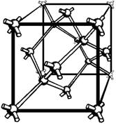
Figure 1-7 - a typical crystal structure.

Figure 1-8 - a two-dimensional view of a silicon cubic lattice.
Silicon and germanium, for example, are the most frequently used semiconductors.
Both are quite similar in their structure and chemical behavior. Each has four electrons
in the valence shell. Consider just silicon. Since it has fewer than the required
number of eight electrons needed in the outer shell, its atoms will unite with other
atoms until eight electrons are shared. This gives each atom a total of eight electrons
in its valence shell; four of its own and four that it borrowed from the surrounding
atoms. The sharing of valence electrons between two or more atoms produces a COVALENT
BOND between the atoms. It is this bond that holds the atoms together in an orderly
structure called a Crystal. a crystal is just another name for a solid whose atoms
or molecules are arranged in a three-dimensional geometrical pattern commonly referred
to as a lattice. Figure 1-7 shows a typical crystal structure. Each sphere in the
figure represents the nucleus of an atom, and the arms that join the atoms and support
the structure are the covalent bonds.
As a result of this sharing process, the valence electrons are held tightly together.
This can best be illustrated by the two-dimensional view of the silicon lattice
in figure 1-8. The circles in the figure represent the nuclei of the atoms. The
+4 in the circles is the net charge of the nucleus plus the inner shells (minus
the valence shell). The short lines indicate valence electrons. Because every atom
in this pattern is bonded to four other atoms, the electrons are not free to move
within the crystal. As a result of this bonding, pure silicon and germanium are
poor conductors of electricity. The reason they are not insulators but semiconductors
is that with the proper application of heat or electrical pressure, electrons can
be caused to break free of their bonds and move into the conduction band. Once in
this band, they wander aimlessly through the crystal.
Q13. What determines the chemical activity of an atom?
Q14. What is the term used to describe the sharing of valence electrons
between two or more atoms?
CONDUCTION PROCESS
As stated earlier, energy can be added to electrons by applying heat. When enough
energy is absorbed by the valence electrons, it is possible for them to break some
of their covalent bonds. Once the bonds are broken, the electrons move to the conduction
band where they are capable of supporting electric current. When a voltage is applied
to a crystal containing these conduction band electrons, the electrons move through
the crystal toward the applied voltage. This movement of electrons in a semiconductor
is referred to as electron current flow.
There is still another type of current in a pure semiconductor. This current
occurs when a covalent bond is broken and a vacancy is left in the atom by the missing
valence electron. This vacancy is commonly referred to as a "hole." The hole is
considered to have a positive charge because its atom is deficient by one electron,
which causes the protons to outnumber the electrons. As a result of this hole, a
chain reaction begins when a nearby electron breaks its own covalent bond to fill
the hole, leaving another hole. Then another electron breaks its bond to fill the
previous hole, leaving still another hole. Each time an electron in this process
fills a hole, it enters into a covalent bond. Even though an electron has moved
from one covalent bond to another, the most important thing to remember is that
the hole is also moving. Therefore, since this process of conduction resembles the
movement of holes rather than electrons, it is termed hole flow (short for hole
current flow or conduction by holes). Hole flow is very similar to electron flow
except that the holes move toward a negative potential and in an opposite direction
to that of the electron. Since hole flow results from the breaking of covalent bonds,
which are at the valence band level, the electrons associated with this type of
conduction contain only valence band energy and must remain in the valence band.
However, the electrons associated with electron flow have conduction band energy
and can, therefore, move throughout the crystal. a good analogy of hole flow is
the movement of a hole through a tube filled with balls (figure 1-9).
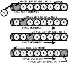
Figure 1-9 - Analogy of hole flow.
When ball number 1 is removed from the tube, a hole is left. This hole is then
filled by ball number 2, which leaves still another hole. Ball number 3 then moves
into the hole left by ball number 2. This causes still another hole to appear where
ball 3 was. Notice the holes are moving to the right side of the tube. This action
continues until all the balls have moved one space to the left in which time the
hole moved eight spaces to the right and came to rest at the right-hand end of the
tube.
In the theory just described, two current carriers were created by the breaking
of covalent bonds: the negative electron and the positive hole. These carriers are
referred to as electron-hole pairs. Since the semiconductor we have been discussing
contains no impurities, the number of holes in the electron-hole pairs is always
equal to the number of conduction electrons. Another way of describing this condition
where no impurities exist is by saying the semiconductor is INTRINSIC. The term
intrinsic is also used to distinguish the pure semiconductor that we have been working
with from one containing impurities.
Q15. Name the two types of current flow in a semiconductor.
Q16. What is the name given to a piece of pure semiconductor material
that has an equal number of electrons and holes?
DOPING PROCESS
The pure semiconductor mentioned earlier is basically neutral. It contains no
free electrons in its conduction bands. Even with the application of thermal energy,
only a few covalent bonds are broken, yielding a relatively small current flow.
A much more efficient method of increasing current flow in semiconductors is by
adding very small amounts of selected additives to them, generally no more than
a few parts per million. These additives are called impurities and the process of
adding them to crystals is referred to as DOPING. The purpose of semiconductor doping
is to increase the number of free charges that can be moved by an external applied
voltage. When an impurity increases the number of free electrons, the doped semiconductor
is Negative or N TYPE, and the impurity that is added is known as an N-type impurity.
However, an impurity that reduces the number of free electrons, causing more
holes, creates a Positive or P-TYPE semiconductor, and the impurity that was
added to it is known as a P-type impurity. Semiconductors which are doped in this
manner - either with N- or P-type impurities - are referred to as EXTRINSIC semiconductors.
N-Type Semiconductor

Figure 1-10 - Germanium crystal doped with arsenic.
The N-type impurity loses its extra valence electron easily when added to a semiconductor
material, and in so doing, increases the conductivity of the material by contributing
a free electron. This type of impurity has 5 valence electrons and is called a PENTAVALENT
impurity. Arsenic, antimony, bismuth, and phosphorous are pentavalent impurities.
Because these materials give or donate one electron to the doped material, they
are also called DONOR impurities.
When a pentavalent (donor) impurity, like arsenic, is added to germanium, it
will form covalent bonds with the germanium atoms. Figure 1-10 illustrates this
by showing an arsenic atom (AS) in a germanium (GE) lattice structure. Notice the
arsenic atom in the center of the lattice. It has 5 valence electrons in its outer
shell but uses only 4 of them to form covalent bonds with the germanium atoms, leaving
1 electron relatively free in the crystal structure. Pure germanium may be converted
into an N-type semiconductor by "doping" it with any donor impurity having 5 valence
electrons in its outer shell. Since this type of semiconductor (N-type) has a surplus
of electrons, the electrons are considered MAJORITY carriers, while the holes, being
few in number, are the MINORITY carriers.
P-Type Semiconductor
The second type of impurity, when added to a semiconductor material, tends to
compensate for its deficiency of 1 valence electron by acquiring an electron from
its neighbor. Impurities of this type have only 3 valence electrons and are called
TRIVALENT impurities. Aluminum, indium, gallium, and boron are trivalent impurities.
Because these materials accept 1 electron from the doped material, they are also
called ACCEPTOR impurities.
A trivalent (acceptor) impurity element can also be used to dope germanium. In
this case, the impurity is 1 electron short of the required amount of electrons
needed to establish covalent bonds with 4 neighboring atoms. Thus, in a single covalent
bond, there will be only 1 electron instead of 2. This arrangement leaves a hole
in that covalent bond. Figure 1-11 illustrates this theory by showing what happens
when germanium is doped with an indium (In) atom. Notice, the indium atom in the
figure is 1

Figure 1-11. - Germanium crystal doped with indium.
electron short of the required amount of electrons needed to form covalent bonds
with 4 neighboring atoms and, therefore, creates a hole in the structure. Gallium
and boron, which are also trivalent impurities, exhibit these same characteristics
when added to germanium. The holes can only be present in this type semiconductor
when a trivalent impurity is used. Note that a hole carrier is not created by the
removal of an electron from a neutral atom, but is created when a trivalent impurity
enters into covalent bonds with a tetravalent (4 valence electrons) crystal structure.
The holes in this type of semiconductor (P-type) are considered the MAJORITY carriers
since they are present in the material in the greatest quantity. The electrons,
on the other hand, are the MINORITY carriers.
Q17. What is the name given to a doped germanium crystal with an
excess of free holes?
Q18. What are the majority carriers in an N-type semiconductor?
SEMICONDUCTOR DIODE
If we join a section of N-type semiconductor material with a similar section
of P-type semiconductor material, we obtain a device known as a PN JUNCTION. (The
area where the N and P regions meet is appropriately called the junction.) The usual
characteristics of this device make it extremely useful in electronics as a diode
rectifier. The diode rectifier or PN junction diode performs the same function as
its counterpart in electron tubes but in a different way. The diode is nothing more
than a two-element semiconductor device that makes use of the rectifying properties
of a PN junction to convert alternating current into direct current by permitting
current flow in only one direction. The schematic symbol of a PN junction diode
is shown in figure 1-12. The vertical bar represents the cathode (N-type material)
since it is the source of electrons and the arrow represents the anode. (P-type
material) since it is the destination of the electrons. The label "CR1" is an alphanumerical
code used to identify the diode. In this figure, we have only one diode so it is
labeled CR1 (crystal rectifier number one). If there were four diodes shown in the
diagram, the last diode would be labeled CR4. The heavy dark line shows electron
flow. Notice it is against the arrow. For further clarification, a pictorial diagram
of a PN junction and an actual semiconductor (one of many types) are also illustrated.
CONSTRUCTION
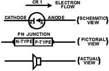
Figure 1-12 - The PN junction diode.
<missing>
Figure 1-13 - Grown and fused PN junctions from which bars are
cut.
Merely pressing together a section of P material and a section of N material,
however, is not sufficient to produce a rectifying junction. The semiconductor should
be in one piece to form a proper PN junction, but divided into a P-type impurity
region and an N-type impurity region. This can be done in various ways. One way
is to mix P-type and N-type impurities into a single crystal during the manufacturing
process. By so doing, a P-region is grown over part of a semiconductor's length
and N- region is grown over the other part. This is called a GROWN junction and
is illustrated in view a of figure 1-13. Another way to produce a PN junction is
to melt one type of impurity into a semiconductor of the opposite type impurity.
For example, a pellet of acceptor impurity is placed on a wafer of N-type germanium
and heated. Under controlled temperature conditions, the acceptor impurity fuses
into the wafer to form a P-region within it, as shown in view B of figure 1-13.
This type of junction is known as an ALLOY or FUSED-ALLOY junction, and is one of
the most commonly used junctions. In figure 1-14, a Point-CONTACT type of construction
is shown. It consists of a fine metal wire, called a cat whisker, that makes contact
with a small area on the surface of an N-type semiconductor as shown in view a of
the figure. The PN union is formed in this process by momentarily applying a high-surge
current to the wire and the N-type semiconductor. The heat generated by this current
converts the material nearest the point of contact to a P-type material (view B).
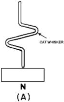
Figure 1-14A - The point-contact type of diode construction.

Figure 1-14B - The point-contact type of diode construction.
Still another process is to heat a section of semiconductor material to near
melting and then diffuse impurity atoms into a surface layer. Regardless of the
process, the objective is to have a perfect bond everywhere along the union (interface)
between P and N materials. Proper contact along the union is important because,
as we will see later, the union (junction or interface) is the rectifying agent
in the diode.
Q19. What is the purpose of a PN junction diode?
Q20. In reference to the schematic symbol for a diode, do electrons
flow toward or away from the arrow?
Q21. What type of PN diode is formed by using a fine metal wire and
a section of N-type semiconductor material?
PN JUNCTION Operation
Now that you are familiar with P- and N-type materials, how these materials are
joined together to form a diode, and the function of the diode, let us continue
our discussion with the operation of the PN junction. But before we can understand
how the PN junction works, we must first consider current flow in the materials
that make up the junction and what happens initially within the junction when these
two materials are joined together.
Current Flow in the N-Type Material

Figure 1-15. - Current flow In the N-type material.
Conduction in the N-type semiconductor, or crystal, is similar to conduction
in a copper wire. That is, with voltage applied across the material, electrons will
move through the crystal just as current would flow in a copper wire. This is shown
in figure 1-15. The positive potential of the battery will attract the free electrons
in the crystal. These electrons will leave the crystal and flow into the positive
terminal of the battery. As an electron leaves the crystal, an electron from the
negative terminal of the battery will enter the crystal, thus completing the current
path. Therefore, the majority current carriers in the N-type material (electrons)
are repelled by the negative side of the battery and move through the crystal toward
the positive side of the battery.
Current Flow in the P-Type Material
Current flow through the P-type material is illustrated in figure 1-16. Conduction
in the P material is by positive holes, instead of negative electrons. a hole moves
from the positive terminal of the P material to the negative terminal. Electrons
from the external circuit enter the negative terminal of the material and fill holes
in the vicinity of this terminal. At the positive terminal, electrons are removed
from the covalent bonds, thus creating new holes. This process continues as the
steady stream of holes (hole current) moves toward the negative terminal.
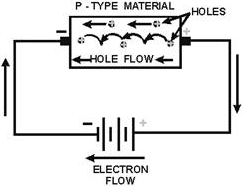
Figure 1-16 - Current flow In the P-type material.
Notice in both N-type and P-type materials, current flow in the external circuit
consists of electrons moving out of the negative terminal of the battery and into
the positive terminal of the battery. Hole flow, on the other hand, only exists
within the material itself.
Q22. What are the majority carriers in a P-type semiconductor?
Q23. Conduction in which type of semiconductor material is similar
to conduction in a copper wire?
Junction Barrier
Although the N-type material has an excess of free electrons, it is still electrically
neutral. This is because the donor atoms in the N material were left with positive
charges after free electrons became available by covalent bonding (the protons outnumbered
the electrons). Therefore, for every free electron in the N material, there is a
corresponding positively charge atom to balance it. The end result is that the N
material has an overall charge of zero.
By the same reasoning, the P-type material is also electrically neutral because
the excess of holes in this material is exactly balanced by the number of electrons.
Keep in mind that the holes and electrons are still free to move in the material
because they are only loosely bound to their parent atoms.
It would seem that if we joined the N and P materials together by one of the
processes mentioned earlier, all the holes and electrons would pair up. On the contrary,
this does not happen. Instead the electrons in the N material diffuse (move or spread
out) across the junction into the P material and fill some of the holes. At the
same time, the holes in the P material diffuse across the junction into the N material
and are filled by N material electrons. This process, called JUNCTION RECombination,
reduces the number of free electrons and holes in the vicinity of the junction.
Because there is a depletion, or lack of free electrons and holes in this area,
it is known as the DEPLETION REGION.
The loss of an electron from the N-type material created a positive ion in the
N material, while the loss of a hole from the P material created a negative ion
in that material. These ions are fixed in place in the crystal lattice structure
and cannot move. Thus, they make up a layer of fixed charges on the two sides of
the junction as shown in figure 1-17. On the N side of the junction, there is a
layer of positively charged ions; on the P side of the junction, there is a layer
of negatively charged ions. An electrostatic field, represented by a small battery
in the figure, is established across the junction between the oppositely

Figure 1-17. - The PN junction barrier formation.
charged ions. The diffusion of electrons and holes across the junction will continue
until the magnitude of the electrostatic field is increased to the point where the
electrons and holes no longer have enough energy to overcome it, and are repelled
by the negative and positive ions respectively. At this point equilibrium is established
and, for all practical purposes, the movement of carriers across the junction ceases.
For this reason, the electrostatic field created by the positive and negative ions
in the depletion region is called a barrier.
The action just described occurs almost instantly when the junction is formed.
Only the carriers in the immediate vicinity of the junction are affected. The carriers
throughout the remainder of the N and P material are relatively undisturbed and
remain in a balanced condition.
forWARD BIAS. - An external voltage applied to a PN junction
is call BIAS. If, for example, a battery is used to supply bias to a PN junction
and is connected so that its voltage opposes the junction field, it will reduce
the junction barrier and, therefore, aid current flow through the junction. This
type of bias is known as forward bias, and it causes the junction to offer only
minimum resistance to the flow of current.
Forward bias is illustrated in figure 1-18. Notice the positive terminal of the
bias battery is connected to the P-type material and the negative terminal of the
battery is connected to the N-type material. The positive potential repels holes
toward the junction where they neutralize some of the negative ions. At the same
time the negative potential repels electrons toward the junction where they neutralize
some of the positive ions. Since ions on both sides of the barrier are being neutralized,
the width of the barrier decreases. Thus, the effect of the battery voltage in the
forward-bias direction is to reduce the barrier potential across the junction and
to allow majority carriers to cross the junction. Current flow in the forward-biased
PN junction is relatively simple. An electron leaves the negative terminal of the
battery and moves to the terminal of the N-type material. It enters the N material,
where it is the majority carrier and moves to the edge of the junction barrier.
Because of forward bias, the barrier offers less opposition to the electron and
it will pass through the depletion region into the P-type material. The electron
loses energy in overcoming the opposition of the junction barrier, and upon entering
the P material, combines with a hole. The hole was produced when an electron was
extracted from the P material by the positive potential of the battery. The created
hole moves through the P material toward the junction where it combines with an
electron.
| - |
Matter, Energy,
and Direct Current |
| - |
Alternating Current and Transformers |
| - |
Circuit Protection, Control, and Measurement |
| - |
Electrical Conductors, Wiring Techniques,
and Schematic Reading |
| - |
Generators and Motors |
| - |
Electronic Emission, Tubes, and Power Supplies |
| - |
Solid-State Devices and Power Supplies |
| - |
Amplifiers |
| - |
Wave-Generation and Wave-Shaping Circuits |
| - |
Wave Propagation, Transmission Lines, and
Antennas |
| - |
Microwave Principles |
| - |
Modulation Principles |
| - |
Introduction to Number Systems and Logic Circuits |
| - |
- Introduction to Microelectronics |
| - |
Principles of Synchros, Servos, and Gyros |
| - |
Introduction to Test Equipment |
| - |
Radio-Frequency Communications Principles |
| - |
Radar Principles |
| - |
The Technician's Handbook, Master Glossary |
| - |
Test Methods and Practices |
| - |
Introduction to Digital Computers |
| - |
Magnetic Recording |
| - |
Introduction to Fiber Optics |
| Note: Navy Electricity and Electronics Training
Series (NEETS) content is U.S. Navy property in the public domain. |
|