Module 7 - Introduction to Solid-State Devices and Power Supplies
Pages i ,
1-1,
1-11,
1-21,
1-31,
1-41,
2-1,
2-11,
2-21,
2-31,
2-41,
2-51,
3-1,
3-11,
3-21,
3-31,
3-41,
3-51,
4-1 to 4-10,
4-11,
4-21,
4-31,
4-41,
4-51, Index
Amplifier ClassES
of Operation In the previous discussions, we assumed that for every portion of the input signal
there was an output from the amplifier. This is not always the case with amplifiers. It may be desirable to have
the transistor conducting for only a portion of the input signal. The portion of the input for which there is an
output determines the class of operation of the amplifier. There are four classes of amplifier operations. They
are class A, class AB, class B, and class C. Class a Amplifier Operation Class a
amplifiers are biased so that variations in input signal polarities occur within the limits of CUTofF and
SATURATION. In a PNP transistor, for example, if the base becomes positive with respect to the emitter, holes will
be repelled at the PN junction and no current can flow in the collector circuit. This condition is known as
cutoff. Saturation occurs when the base becomes so negative with respect to the emitter that changes in the signal
are not reflected in collector-current flow. Biasing an amplifier in this manner places the dc operating
point between cutoff and saturation and allows collector current to flow during the complete cycle (360 degrees)
of the input signal, thus providing an output which is a replica of the input. Figure 2-12 is an example of a
class a amplifier. Although the output from this amplifier is 180 degrees out of phase with the input, the output
current still flows for the complete duration of the input. The class a operated amplifier is used as an
audio- and radio-frequency amplifier in radio, radar, and sound systems, just to mention a few examples.
For a comparison of output signals for the different amplifier classes of operation, refer to figure 2-15 during
the following discussion.

Figure 2-15. - a comparison of output signals for the different amplifier classes of operation. 2-21
Class AB Amplifier Operation Amplifiers designed for class AB operation are
biased so that collector current is zero (cutoff) for a portion of one alternation of the input signal. This is
accomplished by making the forward-bias voltage less than the peak value of the input signal. By doing this, the
base-emitter junction will be reverse biased during one alternation for the amount of time that the input signal
voltage opposes and exceeds the value of forward-bias voltage. Therefore, collector current will flow for more
than 180 degrees but less than 360 degrees of the input signal, as shown in figure 2-15 view B. As compared to the
class a amplifier, the dc operating point for the class AB amplifier is closer to cutoff. The class AB
operated amplifier is commonly used as a push-pull amplifier to overcome a side effect of class B operation called
crossover distortion.
Class B Amplifier Operation Amplifiers biased so that collector current is cut
off during one-half of the input signal are classified class B. The dc operating point for this class of amplifier
is set up so that base current is zero with no input signal. When a signal is applied, one half cycle will forward
bias the base-emitter junction and IC will flow. The other half cycle will reverse bias the base-emitter junction
and IC will be cut off. Thus, for class B operation, collector current will flow for approximately 180 degrees
(half) of the input signal, as shown in figure 2-15 view C. The class B operated amplifier is used
extensively for audio amplifiers that require high-power outputs. It is also used as the driver- and
power-amplifier stages of transmitters. Class C Amplifier Operation In class C
operation, collector current flows for less than one half cycle of the input signal, as shown in figure 2-15 view
D. The class C operation is achieved by reverse biasing the emitter-base junction, which sets the dc operating
point below cutoff and allows only the portion of the input signal that overcomes the reverse bias to cause
collector current flow.
The class C operated amplifier is used as a radio-frequency amplifier in transmitters. From the previous
discussion, you can conclude that two primary items determine the class of operation of an amplifier - (1) the
amount of bias and (2) the amplitude of the input signal. With a given input signal and bias level, you can change
the operation of an amplifier from class a to class B just by removing forward bias. Also, a class a amplifier can
be changed to class AB by increasing the input signal amplitude. However, if an input signal amplitude is
increased to the point that the transistor goes into saturation and cutoff, it is then called an OVERDRIVEN
amplifier. You should be familiar with two terms used in conjunction with amplifiers - Fidelity and
Efficiency. Fidelity is the faithful reproduction of a signal. In other words, if the output of an amplifier is
just like the input except in amplitude, the amplifier has a high degree of fidelity. The opposite of fidelity is
a term we mentioned earlier - distortion. Therefore, a circuit that has high fidelity has low distortion. In
conclusion, a class a amplifier has a high degree of fidelity. a class AB amplifier has less fidelity, and class B
and class C amplifiers have low or "poor" fidelity. The efficiency of an amplifier refers to the ratio of
output-signal power compared to the total input power. An amplifier has two input power sources: one from the
signal, and one from the power supply. Since every device takes power to operate, an amplifier that operates for
360 degrees of the input signal uses more power than if operated for 180 degrees of the input signal. By using
more power, an amplifier has less power available for the output signal; thus the efficiency of the amplifier is
low. This is the case
2-22
with the class a amplifier. It operates for 360 degrees of the input signal and requires a relatively
large input from the power supply. Even with no input signal, the class a amplifier still uses power from the
power supply. Therefore, the output from the class a amplifier is relatively small compared to the total input
power. This results in low efficiency, which is acceptable in class a amplifiers because they are used where
efficiency is not as important as fidelity. Class AB amplifiers are biased so that collector current is
cut off for a portion of one alternation of the input, which results in less total input power than the class a
amplifier. This leads to better efficiency. Class B amplifiers are biased with little or no collector
current at the dc operating point. With no input signal, there is little wasted power. Therefore, the efficiency
of class B amplifiers is higher still. The efficiency of class C is the highest of the four classes of
amplifier operations.
Q22. What amplifier class of operation allows collector current to flow during the complete cycle of
the input? Q23. What is the name of the term used to describe the condition in a transistor when the
emitter-base junction has zero bias or is reverse biased and there is no collector current?
Q24. What two primary items determine the class of operation of an amplifier? Q25. What amplifier
class of operation is the most inefficient but has the least distortion? Transistor ConfigurationS
A transistor may be connected in any one of three basic configurations (fig. 2-16): common emitter (CE),
common base (CB), and common collector (CC). The term common is used to denote the element that is common to both
input and output circuits. Because the common element is often grounded, these configurations are frequently
referred to as grounded emitter, grounded base, and grounded collector.
2-23

Figure 2-16. - Transistor configurations. Each configuration, as you will see later, has particular characteristics that make it suitable for
specific applications. An easy way to identify a specific transistor configuration is to follow three simple
steps:
1. Identify the element (emitter, base, or collector) to which the input signal is applied.
2. Identify the element (emitter, base, or collector) from which the output signal is taken. 3. The
remaining element is the common element, and gives the configuration its name. Therefore, by applying
these three simple steps to the circuit in figure 2-12, we can conclude that this circuit is more than just a
basic transistor amplifier. It is a common-emitter amplifier.
Common Emitter The common-emitter configuration (CE) shown in figure 2-16 view a is the
arrangement most frequently used in practical amplifier circuits, since it provides good voltage, current, and
power gain. The common emitter also has a somewhat low input resistance (500 ohms-1500 ohms), because the input is
applied to the forward-biased junction, and a moderately high output resistance (30 kilohms-50 kilohms or more),
because the output is taken off the reverse-biased junction. Since the input signal is applied to the base-emitter
circuit and the output is taken from the collector-emitter circuit, the emitter is the element common to both
input and output.
2-24
Since you have already covered what you now know to be a common-emitter amplifier (fig. 2-12), let's take a
few minutes and review its operation, using the PNP common-emitter configuration shown in figure 2-16 view A.
When a transistor is connected in a common-emitter configuration, the input signal is injected between
the base and emitter, which is a low resistance, low-current circuit. As the input signal swings positive, it also
causes the base to swing positive with respect to the emitter. This action decreases forward bias which reduces
collector current (IC) and increases collector voltage (making VC more negative). During the
negative alternation of the input signal, the base is driven more negative with respect to the emitter. This
increases forward bias and allows more current carriers to be released from the emitter, which results in an
increase in collector current and a decrease in collector voltage (making VC less negative or swing in
a positive direction). The collector current that flows through the high resistance reverse-biased junction also
flows through a high resistance load (not shown), resulting in a high level of amplification. Since the
input signal to the common emitter goes positive when the output goes negative, the two signals (input and output)
are 180 degrees out of phase. The common-emitter circuit is the only configuration that provides a phase reversal.
The common-emitter is the most popular of the three transistor configurations because it has the best
combination of current and voltage gain. The term Gain is used to describe the amplification capabilities of the
amplifier. It is basically a ratio of output versus input. Each transistor configuration gives a different value
of gain even though the same transistor is used. The transistor configuration used is a matter of design
consideration. However, as a technician you will become interested in this output versus input ratio (gain) to
determine whether or not the transistor is working properly in the circuit. The current gain in the
common-emitter circuit is called BETA (β). Beta is the relationship of collector current (output current) to base
current (input current). To calculate beta, use the following formula:

(������ is the Greek letter delta, it is used to indicate a small change)
For example, if the input current (IB) in a common emitter changes from 75 uA to 100 uA and
the output current (IC) changes from 1.5 mA to 2.6 mA, the current gain (β) will be 44.
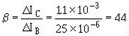
This simply means that a change in base current produces a change in collector current which is 44 times
as large. You may also see the term hfe used in place of b. The terms hfe
and β are equivalent and may be used interchangeably. This is because "hfe" means:
2-25
.................................... h = hybrid (meaning mixture)
.................................... f = forward current transfer ratio
.................................... e = common emitter configuration The resistance gain of the
common emitter can be found in a method similar to the one used for finding beta:

Once the resistance gain is known, the voltage gain is easy to calculate since it is equal to the
current gain (β) multiplied by the resistance gain (E = βR). And, the power gain is equal to the voltage gain
multiplied by the current gain β (P = βE). Common Base The common-base
configuration (CB) shown in figure 2-16, view B is mainly used for impedance matching, since it has a low input
resistance (30 ohms-160 ohms) and a high output resistance (250 kilohms-550 kilohms). However, two factors limit
its usefulness in some circuit applications: (1) its low input resistance and (2) its current gain of less than 1.
Since the CB configuration will give voltage amplification, there are some additional applications, which require
both a low-input resistance and voltage amplification, that could use a circuit configuration of this type; for
example, some microphone amplifiers.
In the common-base configuration, the input signal is applied to the emitter, the output is taken from
the collector, and the base is the element common to both input and output. Since the input is applied to the
emitter, it causes the emitter-base junction to react in the same manner as it did in the common-emitter circuit.
For example, an input that aids the bias will increase transistor current, and one that opposes the bias will
decrease transistor current. Unlike the common-emitter circuit, the input and output signals in the
common-base circuit are in phase. To illustrate this point, assume the input to the PNP version of the common-base
circuit in figure 2-16 view B is positive. The signal adds to the forward bias, since it is applied to the
emitter, causing the collector current to increase. This increase in Ic results in a greater voltage drop across
the load resistor RL
(not shown), thus lowering the collector voltage VC. The collector voltage, in becoming less negative,
is swinging in a positive direction, and is therefore in phase with the incoming positive signal.
The current gain in the common-base circuit is calculated in a method similar to that of the common emitter except
that the input current is IE not IB and the term ALPHA (α) is used in place of beta for gain. Alpha is the relationship of collector current (output current) to emitter current
(input current). Alpha is calculated using the formula:

For example, if the input current (IE) in a common base changes from 1 mA to 3 mA and the
output current (IC) changes from 1 mA to 2.8 mA, the current gain (α)
will be 0.90 or:
2-26

This is a current gain of less than 1. Since part of the emitter current flows into the base
and does not appear as collector current, collector current will always be less than
the emitter current that causes it. (Remember, IE = IB + IC) Therefore, ALPHA is
ALWAYS LESS THAN ONE for a Common-Base Configuration. Another term for "α" is
hf. These terms (and hf) are equivalent and may be used interchangeably. The meaning for the
term hf is derived in the same manner as the term hfe mentioned earlier, except that the
last letter "e" has been replaced with "b" to stand for common- base configuration.
Many transistor manuals and data sheets only list transistor current gain characteristics in terms of b or hfe. To
find alpha (α) when given beta (β), use the following formula to convert b to a for use with the common-base configuration:

To calculate the other gains (voltage and power) in the common-base configuration when the current gain
(α) is known, follow the procedures described earlier under the common-emitter
section. Common Collector The common-collector configuration (CC) shown in
figure 2-16 view C is used mostly for impedance matching. It is also used as a current driver, because of its
substantial current gain. It is particularly useful in switching circuitry, since it has the ability to pass
signals in either direction (bilateral operation). In the common-collector circuit, the input signal is
applied to the base, the output is taken from the emitter, and the collector is the element common to both input
and output. The common collector is equivalent to our old friend the electron-tube cathode follower. Both have
high input and low output resistance. The input resistance for the common collector ranges from 2 kilohms to 500
kilohms, and the output resistance varies from 50 ohms to 1500 ohms. The current gain is higher than that in the
common emitter, but it has a lower power gain than either the common base or common emitter. Like the common base,
the output signal from the common collector is in phase with the input signal. The common collector is also
referred to as an emitter-follower because the output developed on the emitter follows the input signal applied to
the base. Transistor action in the common collector is similar to the operation explained for the common
base, except that the current gain is not based on the emitter-to-collector current ratio, alpha (α).
Instead, it is based on the emitter-to-base current ratio called GAMMA (γ), because
the output is taken off the emitter. Since a small change in base current controls a large change in emitter
current, it is still possible to obtain high current gain in the common collector. However, since the emitter
current gain is offset by the low output resistance, the voltage gain is always less than 1 (unity), exactly as in
the electron-tube cathode follower The common-collector current gain, gamma (γ),
is defined as
2-27

and is related to collector-to-base current gain, beta (β), of the common-emitter circuit by the
formula:

Since a given transistor may be connected in any of three basic configurations, there is a definite
relationship, as pointed out earlier, between alpha (α), beta (β), and gamma (γ).
These relationships are listed again for your convenience:

Take, for example, a transistor that is listed on a manufacturer's data sheet as having an alpha of
0.90. We wish to use it in a common emitter configuration. This means we must find beta. The calculations are:
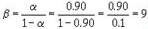
Therefore, a change in base current in this transistor will produce a change in collector current that
will be 9 times as large. If we wish to use this same transistor in a common collector, we can find gamma
(γ) by:

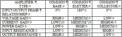
To summarize the properties of the three transistor configurations, a comparison chart is provided in
table 2-1 for your convenience.
Table 2-1. - Transistor Configuration Comparison Chart
 2-28
Now that we have analyzed the basic transistor amplifier in terms of bias, class of operation, and
circuit configuration, let's apply what has been covered to figure 2-12. a reproduction of figure 2-12 is shown
below for your convenience.
 This illustration is not just the basic transistor amplifier shown earlier in figure 2-12 but a class a
amplifier configured as a common emitter using fixed bias. From this, you should be able to conclude the
following:
· Because of its fixed bias, the amplifier is thermally unstable.
· Because of its class a
operation, the amplifier has low efficiency but good fidelity.
· Because it is configured as a common
emitter, the amplifier has good voltage, current, and power gain.
In conclusion, the type of bias, class of operation, and circuit configuration are all clues to the function and
possible application of the amplifier. Q26. What are the three transistor configurations?
Q27. Which transistor configuration provides a phase reversal between the input and output signals?
Q28. What is the input current in the common-emitter circuit? Q29. What is the current gain in a
common-base circuit called? Q30. Which transistor configuration has a current gain of less than 1?
Q31. What is the output current in the common-collector circuit? Q32. Which transistor configuration
has the highest input resistance?
Q33. What is the formula for GAMMA (γ)?
2-29
Transistor SPECIFICATIONS Transistors are available in a large variety of shapes and sizes, each with its own unique
characteristics. The characteristics for each of these transistors are usually presented on SPECIFICATION SHEETS
or they may be included in transistor manuals. Although many properties of a transistor could be specified on
these sheets, manufacturers list only some of them. The specifications listed vary with different manufacturers,
the type of transistor, and the application of the transistor. The specifications usually cover the following
items. 1. a general description of the transistor that includes the following information:
a. The kind of transistor. This covers the material used, such as germanium or silicon; the type of transistor
(NPN or PNP); and the construction of the transistor(whether alloy-junction, grown, or diffused junction, etc.).
b. Some of the common applications for the transistor, such as audio amplifier, oscillator, rf
amplifier, etc. c. General sales features, such as size and packaging mechanical data).
2. The "Absolute Maximum Ratings" of the transistor are the direct voltage and current values that if exceeded
in operation may result in transistor failure. Maximum ratings usually include collector-to-base voltage,
emitter-to-base voltage, collector current, emitter current, and collector power dissipation. 3. The
typical operating values of the transistor. These values are presented only as a guide. The values vary widely,
are dependent upon operating voltages, and also upon which element is common in the circuit. The values listed
may include collector-emitter voltage, collector current, input resistance, load resistance, current-transfer
ratio (another name for alpha or beta), and collector cutoff current, which is leakage current from collector to
base when no emitter current is applied. Transistor characteristic curves may also be included in this section. a
transistor characteristic curve is a graph plotting the relationship between currents and voltages in a circuit.
More than one curve on a graph is called a "family of curves." 4. Additional information for
engineering-design purposes. So far, many letter symbols, abbreviations, and terms have been introduced,
some frequently used and others only rarely used. For a complete list of all semiconductor letter symbols and
terms, refer to EIMB series 000-0140, Section III.
Transistor IDENTIFICATION Transistors can be identified by a Joint Army-Navy (JAN) designation printed directly on the case of the
transistor. The marking scheme explained earlier for diodes is also used for transistor identification. The first
number indicates the number of junctions. The letter "N" following the first number tells us that the component is
a semiconductor. And, the 2- or 3-digit number following the N is the manufacturer's identification number. If the
last number is followed by a letter, it indicates a later, improved version of the device. For example, a
semiconductor designated as type 2N130A signifies a three-element transistor of semiconductor material that is an
improved version of type 130:
2-30
| - |
Matter, Energy,
and Direct Current |
| - |
Alternating Current and Transformers |
| - |
Circuit Protection, Control, and Measurement |
| - |
Electrical Conductors, Wiring Techniques,
and Schematic Reading |
| - |
Generators and Motors |
| - |
Electronic Emission, Tubes, and Power Supplies |
| - |
Solid-State Devices and Power Supplies |
| - |
Amplifiers |
| - |
Wave-Generation and Wave-Shaping Circuits |
| - |
Wave Propagation, Transmission Lines, and
Antennas |
| - |
Microwave Principles |
| - |
Modulation Principles |
| - |
Introduction to Number Systems and Logic Circuits |
| - |
- Introduction to Microelectronics |
| - |
Principles of Synchros, Servos, and Gyros |
| - |
Introduction to Test Equipment |
| - |
Radio-Frequency Communications Principles |
| - |
Radar Principles |
| - |
The Technician's Handbook, Master Glossary |
| - |
Test Methods and Practices |
| - |
Introduction to Digital Computers |
| - |
Magnetic Recording |
| - |
Introduction to Fiber Optics |
| Note: Navy Electricity and Electronics Training
Series (NEETS) content is U.S. Navy property in the public domain. |
|