Module 11 - Microwave Principles Pages
i,
1-1, 1-11,
1-21,
1-31,
1-41,
1-51,
1-61,
2-1,
2-11, 2-21,
2-31,
2-41,
2-51,
2-61,
3-1,
3-11,
AI-1,
Index-1,
Assignment 1,
Assignment 2
...Pages 1-41 through 1-50
Q-53. What limits the usefulness of high-gain, tunnel-diode frequency converters?
Q-54. The varactor is a PN junction that acts as what type of electronic device?
Q-55. The underlying principle of operation of the parametric amplifier is based
on what property?
Q-56. What is the most important feature of the parametric amplifier?
Q-57. How is amplification achieved in the circuit shown in figure 2-43?
Q-58. What is the purpose of the pump in a parametric amplifier?
Q-59. The pump signal frequency must be of what value when compared to the input
signal of a simple parametric amplifier?
Q-60. What is the primary difference between the pump signal of a simple parametric
amplifier and the pump signal of a nondegenerative parametric amplifier?
Q-61. In a nondegenerative parametric amplifier the difference between the input
frequency and the pump frequency is called what?
Bulk-Effect Semiconductors are unlike normal pn-junction diodes
in both construction and operation. Some types have no junctions and the processes
necessary for operation occur in a solid block of semiconductor material. Other
types have more than one junction but still use bulk-effect action. Bulk-effect
devices are among the latest of developments in the field of microwave semiconductors
and new applications are being developed rapidly. They seem destined to revolutionize
the field of high- power, solid-state microwave generation because they can produce
much larger microwave power outputs than any currently available pn-junction semiconductors.
Bulk-effect semiconductors are of two basic types: the transferred-electron devices
and the avalanche transit-time devices.
Transferred-Electron Semiconductors

Figure 2-48 - Characteristic curve for a bulk-effect semiconductor.
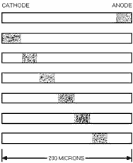
Figure 2-49 - Gallium-arsenide semiconductor domain movement.
The discovery that microwaves could be generated by applying a steady voltage
across a chip of n-type gallium-arsenide (GaAs) crystal was made in 1963 by J.B.
Gunn. The device is operated by raising electrons in the crystal to conduction-band
energy levels that are higher than the level they normally occupy. The overall effect
is called the transferred-electron effect.
In a gallium-arsenide semiconductor, empty electron conduction bands exist that
are at a higher energy level than the conduction bands occupied by most of the electrons.
Any electrons that do occupy the higher conduction band essentially have no mobility.
If an electric field of sufficient intensity is applied to the semiconductor electrons,
they will move from the low-energy conduction band to the high- energy conduction
band and become essentially immobile. The immobile electrons no longer contribute
to the current flow and the applied voltage progressively increases the rate at
which the electrons move from the low band to the high band. As the curve in figure
2-48 shows, the maximum current rate is reached and begins to decrease even though
the applied voltage continues to increase. The point at which the current on the
curve begins to decrease is called the THRESHOLD. This point is the beginning of
the negative-resistance region. Negative resistance is caused by electrons moving
to the higher conduction band and becoming immobile.
If an increase in voltage is applied to a gallium-arsenide semiconductor, which
is biased to operate in the negative-resistance region, it divides into regions
of varying electric fields. a tiny region, known as a DOMAIN, forms that has an
electric field of much greater intensity than the fields in the rest of the semiconductor.
The applied voltage causes the domain to travel across the semiconductor chip from
the cathode to the anode. The high field intensity of the domain is caused by the
interaction of the slow electrons in the high-energy band and the faster electrons
in the low-energy band. The electrons in the low-energy band travel faster than
the moving domain and continually catch up during the transit from cathode to anode.
When the fast electrons catch up to the domain, the high field intensity forces
them into the higher band where they lose most of their mobility. This also causes
them to fall behind the moving domain. Random scattering causes the electrons to
lose some energy and drop back into the lower, faster, energy band and race again
after the moving domain. The movement from the low-energy band to the high-energy
band causes the electrons to bunch up at the back of the domain and to provide the
electron- transfer energy that creates the high field intensity in the domain. The
domains form at or near the cathode and move across the semiconductor to the anode,
as shown in figure 2-49. As the domain disappears at the anode, a new domain forms
near the cathode and repeats the process.
The Gunn Oscillator is a source of microwave energy that uses
the bulk-effect, gallium- arsenide semiconductor. The basic frequency of a Gunn
oscillator is inversely proportional to the transit time of a domain across the
semiconductor. The transit time is proportional to the length of semiconductor
material, and to some extent, the voltage applied. Each domain causes a pulse of
current at the output; thus, the output is a frequency determined by the physical
length of the semiconductor chip.
The Gunn oscillator can deliver continuous power up to about 65 milliwatts and
pulsed outputs of up to about 200 watts peak. The power output of a solid chip is
limited by the difficulty of removing heat from the small chip. Much higher power
outputs have been achieved using wafers of gallium-arsenide as a single source.
Avalanche Transit-Time Diodes
Avalanche transit-time diodes, also called IMPATT (Impact Avalanche and Transit-Time)
diodes, are multilayer diodes of several different types used to generate microwave
power. The earliest of the avalanche transit-time diodes consists of four layers
in a PNIN arrangement. The intrinsic (I) layer has neither p nor n properties.
The PN junction for the PNIN diode, shown in figure 2-50, is strongly reverse
biased to cause an avalanche in its depletion layer when the positive half cycle
of a microwave signal is applied. The avalanche effect causes the electrons in the
n region, which is very thin, to cross over to the intrinsic layer. The intrinsic
layer is constructed so that the drift transit time causes the current to lag the
signal voltage by more than 90 degrees at the desired frequency. Such a lag represents
a negative resistance at the desired frequency. The PNIN avalanche transit-time
diode, when inserted in a microwave cavity with the proper dc bias, amplifies microwave
signals introduced to the cavity.
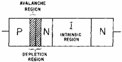
Figure 2-50. - Avalanche transit time for a PNIN diode.
More recent research has shown that pin-junction diodes and simple PN-junction
diodes can show negative resistance and amplification at microwave frequencies when
they are reverse biased into an avalanche condition. The negative resistance in
a simple PN-junction or pin diode is the result of a more complicated internal mechanism
than in the PNIN diode. The avalanche region and the drift region of the PNIN diode
are physically separate. Diodes of the PN and pin type must use the same physical
region for both avalanche and drift-time control. In all types of avalanche transit-time
diodes, the negative-resistance property causes dc bias energy to be absorbed by
electrons in the avalanche process and given up to the applied microwave field.
Q-62. What is the output frequency of an upper-sideband parametric-frequency
converter?
Q-63. What is the primary advantage of bulk-effect devices over normal PN-junction
semiconductors?
Q-64. What happens to the electrons of a gallium-arsenide semiconductor when
they move from the normal low-energy conduction band to the high-energy conduction
band?
Q-65. The point on the current curve of a gallium-arsenide semiconductor at which
it begins to exhibit negative resistance is called what?
Q-66. The domain in a gallium-arsenide semiconductor has what type of electrical
field when compared to the other regions across the body of a semiconductor?
Q-67. What characteristic of a Gunn oscillator is inversely proportional to the
transit time of the domain across the semiconductor?
Q-68. What is the junction arrangement of the original avalanche transit-time
diode?
Q-69. What causes dc bias energy to be absorbed by avalanche electrons and given
up to the microwave field applied to an avalanche transit-time diode?
The Point-Contact Diode
Point-Contact Diodes, commonly called CrystalS, are the oldest
microwave semiconductor devices. They were developed during World War II for use
in microwave receivers and are still in widespread use as receiver mixers and detectors.
Unlike the PN-junction diode, the point-contact diode depends on the pressure
of contact between a point and a semiconductor crystal for its operation. Figure
2-51A and B, illustrate a point-contact diode. One section of the diode consists
of a small rectangular crystal of n-type silicon. a fine beryllium-copper, bronze-phosphor,
or tungsten wire called the CATWHIsKER presses against the crystal and forms the
other part of the diode. During the manufacture of the point contact diode, a relatively
large current is passed from the catwhisker to the silicon crystal. The result of
this large current is the formation of a small region of p-type material around
the crystal in the vicinity of the point contact. Thus, a PN-junction is formed
which behaves in the same way as a normal PN-junction.
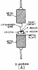
Figure 2-51A. - Point-contact diode. Diagram.
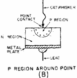
Figure 2-51B. - Point-contact diode. P REGION AROUND Point.
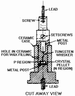
Figure 2-51C. - Point-contact diode. CUT AWAY VIEW.
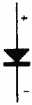
Figure 2-51D. - Point-contact diode. SCHEMATIC SYMBOL.
The pointed wire is used instead of a flat metal plate to produce a high-intensity
electric field at the point contact without using a large external source voltage.
It is not possible to apply large voltages across the average semiconductor because
of the excessive heating.
The end of the catwhisker is one of the terminals of the diode. It has a low-resistance
contact to the external circuit. a flat metal plate on which the crystal is mounted
forms the lower contact of the diode with the external circuit. Both contacts with
the external circuit are low-resistance contacts. The characteristics of the point-contact
diode under forward and reverse bias are somewhat different from those of the junction
diode.
With forward bias, the resistance of the point-contact diode is higher than that
of the junction diode. With reverse bias, the current flow through a point-contact
diode is not as independent of the voltage applied to the crystal as it is in the
junction diode. The point-contact diode has an advantage over the junction diode
because the capacitance between the catwhisker and the crystal is less than the
capacitance between the two sides of the junction diode. As such, the capacitive
reactance existing across the point- contact diode is higher and the capacitive
current that will flow in the circuit at high frequencies is smaller. a cutaway
view of the entire point-contact diode is shown in figure 2-51C. The schematic symbol
of a point-contact diode is shown in figure 2-51D.
Schottky Barrier Diode
The SCHOTTKY BARRIER DIODE is actually a variation of the point-contact diode
in which the metal semiconductor junction is a surface rather than a point contact.
The large contact area, or barrier, between the metal and the semiconductor in the
Schottky barrier diode provides some advantages over the point-contact diode. Lower
forward resistance and lower noise generation are the most important advantages
of the Schottky barrier diode. The applications of the Schottky barrier diode are
the same as those of the point-contact diode. The low noise level generated by Schottky
diodes makes them especially suitable as microwave receiver detectors and mixers.
The Schottky barrier diode is sometimes called the HOT-ELECTRON or HOT-CARRIER
DIODE because the electrons flowing from the semiconductor to the metal have a higher
energy level than the electrons in the metal. The effect is the same as it would
be if the metal were heated to a higher temperature than normal. Figure 2-52 is
an illustration of the construction of a Schottky barrier diode.
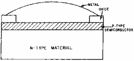
Figure 2-52. - Schottky-barrier diode.
PIN Diodes
The pin diode consists of two narrow, but highly doped, semiconductor regions
separated by a thicker, lightly-doped material called the intrinsic region. As suggested
in the name, pin, one of the heavily doped regions is p-type material and the other
is n-type. The same semiconductor material, usually silicon, is used for all three
areas. Silicon is used most often for its power-handling capability and because
it provides a highly resistive intrinsic (I) region. The pin diode acts as an ordinary
diode at frequencies up to about 100 megahertz, but above this frequency the operational
characteristics change. The large intrinsic region increases the transit time
of electrons crossing the region. Above 100 megahertz, electrons begin to accumulate
in the intrinsic region. The carrier storage in the intrinsic region causes the
diode to stop acting as a rectifier and begin acting as a variable resistance. The
equivalent
circuit of a pin diode at microwave frequencies is shown in figure 2-53A. a resistance
versus voltage characteristic curve is shown in figure 2-53B.

Figure 2-53A. - Diode equivalent circuit (PIN).

Figure 2-53B. - Diode equivalent circuit (PIN).
When the bias on a pin diode is varied, the microwave resistance changes from
a typical value of 6 kilohms under negative bias to about 5 ohms when the bias is
positive. Thus when the diode is mounted across a transmission line or waveguide,
the loading effect is insignificant while the diode is reverse biased, and the diode
presents no interference to power flow. When the diode is forward biased, the resistance
drops to approximately 5 ohms and most power is reflected. In other words, the diode
acts as a switch when mounted in parallel with a transmission line or waveguide.
Several diodes in parallel can switch power in excess of 150 kilowatts peak. The
upper power limit is determined by the ability of the diode to dissipate power.
The upper frequency limit is determined by the shunt capacitance of the PN junction,
shown as C1 in figure 2-53A. Pin diodes with upper limit frequencies in excess of
30 gigahertz are available.
Q-70. During the manufacture of a point-contact diode, what is the purpose of
passing a relatively large current from the catwhisker to the silicon crystal?
Q-71. What is the capacitive reactance across a point-contact diode as compared
to a normal junction diode?
Q-72. What are the most important advantages of the Schottky barrier diode?
Q-73. At frequencies above 100 megahertz, the intrinsic (i) region causes
a pin diode to act as what?
Q-74. The pin diode is primarily used for what purpose?
Microwave Transistors
Transistors, like vacuum tubes, have had a very limited application in the microwave
range. Many of the same problems encountered with vacuum tubes, such as transit-time
effects, also limit the upper frequency range of transistors. However, research
in the area of microwave transistors, and especially Microwave INTEGRATED Circuits
(ICs), is proceeding rapidly.
Gallium-Arsenide FET Amplifiers have been developed which provide
low-noise amplification up to about 30 dB in the 7- to 18-gigahertz range. The power
output of many of these amplifiers is relatively low, approximately 20 to 200 milliwatts,
but that is satisfactory for many microwave applications. Research has extended
both the frequency range and the power output of gallium-arsenide FET amplifiers
to frequencies as high as 26.5 gigahertz and power levels in excess of 1 watt in
multistage amplifiers.
Silicon Silicon Bipolar Transistor Amplifiers in integrated
circuit form have been developed that provide up to 40 watts peak power in the 1-
to 1.5-gigahertz range. Other types of microwave transistor amplifiers combined
into multistage modules are capable of providing power outputs approaching 100 watts.
Microwave transistor amplifiers, because of their stability, light weight, and
long life, are rapidly replacing microwave tubes in the first stages of high-powered
radar and communications transmitters. In the future new systems will be almost
completely solid state.
Summary
The information that follows summarizes the important points presented in this
chapter. The use of microwave frequencies forced the development of special tubes
to offset the limitations caused by interelectrode capacitance, lead inductance,
and electron transit-time effects in conventional tubes. Microwave tubes, such as
the klystron and TWT, take advantage of transit-time effects through the use of
VELOCITY MODULATION to amplify and generate microwave energy.
The KLYSTRON is a velocity-modulated tube which may be used as an amplifier or
oscillator. The klystron, when used as an amplifier, requires at least two resonant
cavities, the buncher and the catcher. a diagram of a basic klystron is shown at
the right.

The REFLEX KLYSTRON, shown at the right, is used only as an oscillator and uses
only one cavity to bunch and collect the electrons. The frequency is determined
by the size and shape of the cavity. The reflex klystron has several possible modes
of operation which are determined by electron transit time. Electron transit time
is controlled by the REPELLER voltage.
Pages 1-61 through 1-68
| - |
Matter, Energy,
and Direct Current |
| - |
Alternating Current and Transformers |
| - |
Circuit Protection, Control, and Measurement |
| - |
Electrical Conductors, Wiring Techniques,
and Schematic Reading |
| - |
Generators and Motors |
| - |
Electronic Emission, Tubes, and Power Supplies |
| - |
Solid-State Devices and Power Supplies |
| - |
Amplifiers |
| - |
Wave-Generation and Wave-Shaping Circuits |
| - |
Wave Propagation, Transmission Lines, and
Antennas |
| - |
Microwave Principles |
| - |
Modulation Principles |
| - |
Introduction to Number Systems and Logic Circuits |
| - |
- Introduction to Microelectronics |
| - |
Principles of Synchros, Servos, and Gyros |
| - |
Introduction to Test Equipment |
| - |
Radio-Frequency Communications Principles |
| - |
Radar Principles |
| - |
The Technician's Handbook, Master Glossary |
| - |
Test Methods and Practices |
| - |
Introduction to Digital Computers |
| - |
Magnetic Recording |
| - |
Introduction to Fiber Optics |
| Note: Navy Electricity and Electronics Training
Series (NEETS) content is U.S. Navy property in the public domain. |
|