|
December 13, 1965 Electronics
 [Table of Contents] [Table of Contents]
Wax nostalgic about and learn from the history of early electronics.
See articles from Electronics,
published 1930 - 1988. All copyrights hereby acknowledged.
|
The December 1965 issue of
Electronics magazine reported in multiple articles on the state of Japan's
electronics industry (see the
table
of contents for other stories). Japan's indisputable lead today in many realms
of semiconductor, commercial, and consumer products proves successful implementation
of the strategy described in these articles. Per this piece's NTT employee authors,
"In one decade, Japan's semiconductor industry has become the world's second largest.
Pioneering engineers, a variety of unusual devices, and breakthroughs in miniaturization
techniques account for phenomenal growth." A notable claim is taking credit for
inventing the ceramic "pill" packaging format for high frequency transistors.
All these articles appeared in this issue:
Westernizing
Japan |
Japanese Technology - The New Push for Technical Leadership |
Japanese Technology - When You're Second, You Try Harder |
Japan Stresses Research |
Japan: An Industrious Competitor
Japanese Technology - When You're Second, You Try Harder

Nippon Electric Co.'s multiple diffused base transistor (left)
compared to a conventional planar transistor at right. By widening the base area
with a second diffusion, NEC reduces base spreading resistance, thus increasing
maximum frequency
In one decade, Japan's semiconductor industry has become the world's second largest.
Pioneering engineers, a variety of unusual devices, and breakthroughs in miniaturization
techniques account for phenomenal growth.
By Takuya Kojima and Makoto Watanabe,
Electrical Communications Laboratory, Nippon Telegraph and Telephone Public Corp.,
Tokyo
Large scale production of semiconductor devices is the nucleus of the Japanese
electronics industry. More than 400 million transistors were produced last year,
making Japan's semiconductor industry the second largest in the world, trailing
only the United States. Yet quantity is not the industry's sole accomplishment.
Japanese engineers have created some unusual devices such as the passivated mesa
transistor, a bidirectional twin transistor, the Esaki diode, and a double-diffused
pnp transistor of unique structure.
All this has happened in the last decade. The dominant force behind such rapid
growth has been Japan's pioneering - in the transistorizing of consumer products
such as a-m and f-m radios, tape recorders and television sets, now small enough
to be called micro sets.
The structure of the Japanese industry helped too. All the makers of semiconductor
devices in Japan - and the total number is less than 20 - also manufacture consumer
products, other electronic equipment or both. Because they are in the same company,
information flows rapidly between device builders and equipment designers.
Most of the semiconductors made in Japan are germanium devices, and go into consumer
products. New consumer products, however, require better quality devices. Thus,
the transistorization of large television reviewers, with screens up to 19 inches,
demands high-frequency transistors and high-power devices. Communication and industrial
equipment also needs special-purpose devices of high quality. Although silicon technology
is new in Japan, its spread has been rapid and most semiconductor suppliers produce
both germanium and silicon devices.

Emitter mesa transistor built by the Nippon Electric Co. (left)
withstands drive-in effect which had destroyed conventional mesa transistor (right).
Challenge of Higher Frequencies
As in the United States, there is great pressure in Japan to produce higher-frequency
devices. For example, television makers want transistors capable of operating up
to 1,000 megacycles for ultrahigh-frequency receivers. For this application, Japanese
suppliers offer both germanium and silicon devices.
To boost operating frequency, Japanese firms are trying either to minimize the
base spreading resistance of their devices or to minimize the collector capacitance.
The reasons become evident from the equation for maximum frequency of oscillation
of a transistor:
 where rbb' is the base spreading resistance,
cc is the collector capacitance and τec is the carrier
transit time between emitter and collector. The base spreading resistance and collector
capacitance degrade performance. Base spreading resistance not only decreases the
power gain and output power but also degrades the noise figure. where rbb' is the base spreading resistance,
cc is the collector capacitance and τec is the carrier
transit time between emitter and collector. The base spreading resistance and collector
capacitance degrade performance. Base spreading resistance not only decreases the
power gain and output power but also degrades the noise figure.
To lower this resistance in silicon transistors, firms have introduced some novel
device structures. For example, the Nippon Electric Co., Japan's biggest microwave
equipment manufacturer, uses a multiple base diffusion process to add another area
of impurities in the 2SC288, 2SC289, and 2SC272 devices (shown above). After the
usual diffusion has formed a conventional base area, a second process diffuses impurities
just outside the emitter area, widening the base thickness and reducing the base
spreading resistance. The rbb'cc product of the 2SC288 is
only 3 picoseconds; the base resistance is less than 1/3 that of a conventional
transistor.
NEC also achieves a low base spreading resistance with a second approach called
emitter mesa structure and shown in the figure below. This structure reduces the
drive-in effect in which impurities in the base region are driven toward the collector
area, forming a small projection in the collector junction plane.
Though the effect is more pronounced in a silicon mesa transistor, where the
impurity is gallium, than in a planar transistor where the impurity is boron, It
becomes critical in any high-frequency transistor. That's because a high-frequency
device has an extremely narrow base width which is a bottleneck in the base region
between the area immediately beneath the emitter junction and the area outside the
junction. The bottleneck causes an appreciable increase in the base resistance and
disturbs the uniform carrier flow in the base area.
In the emitter mesa structure, a mesa formed by a vapor etching process prior
to diffusion, offsets the drive-in effect. The height of the mesa is just enough
to compensate for the depth of the projection that would be formed in the junction
plane by the drive-in phenomenon, Thus an ideal flat junction structure results.
 There is one other advantage of the emitter
mesa structure: it eliminates unwanted parasitic capacitance and carrier injections
around the vertical outside edge of the base. Although these can be ignored in an
ordinary device, they are appreciable in a high-frequency transistor whose emitter
width is 5 microns or less. The parasitic capacitance decreases the high-frequency
amplification factor in the small-current region of the emitter; the excess carrier
injection at the edge decreases the current amplification factor in the large-current
region of the emitter. By using the emitter mesa structure NEC increases the gain
by 3 db throughout the range of emitter current and decreases noise by 0.5
db. There is one other advantage of the emitter
mesa structure: it eliminates unwanted parasitic capacitance and carrier injections
around the vertical outside edge of the base. Although these can be ignored in an
ordinary device, they are appreciable in a high-frequency transistor whose emitter
width is 5 microns or less. The parasitic capacitance decreases the high-frequency
amplification factor in the small-current region of the emitter; the excess carrier
injection at the edge decreases the current amplification factor in the large-current
region of the emitter. By using the emitter mesa structure NEC increases the gain
by 3 db throughout the range of emitter current and decreases noise by 0.5
db.
From the equation for the maximum frequency of oscillation of a transistor (above),
it is clear that frequency can also be increased if collector capacitance is reduced.
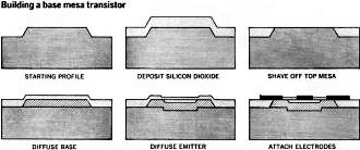
In the base mesa transistor designed by NEC, the geometry lowers this characteristic.
In the structure (p. 83), the base area is defined by a deposited layer of silicon
dioxide. Since only a small region of the base is needed to make contact with the
metallization of the electrode, the capacitance of the metallized portion to the
collector is negligible. Such low collector capacitance makes the device well-suited
for application in wideband-amplifiers - and especially in amplifiers with automatic
gain control because circuit capacitance changes less with changes in voltage stemming
from the gain control.
It seems clear that all three techniques - multiple diffused base, emitter mesa,
and base mesa - could be applied to one device, to produce even better transistors
capable of handling higher frequencies.
At the Matsushita Electronics Corp., the semiconductor producer of the big Matsushita
Industrial Electronics Co., another approach to reducing collector capacitance has
been taken with extended base planar transistors. A highly doped area just beneath
the extended base electrode shields the electrode from the collector. In the Matsushita
2SC562 series, the base-to-collector capacitance is as low as 0.15 picofarads.
Minimum base-to-collector capacitance eliminates several bothersome effects.
By definition, in an extended base electrode device, a metallized contact to the
base is extended along the silicon dioxide layer on top of the collector bulk semiconductor
region for easier bonding of the base lead wire. If the device has an extremely
small base area, the parasitic capacitance between the extended base electrode and
the collector bulk semiconductor region is comparable to the capacitance of the
intrinsic collector junction. Such a high capacitance makes it impossible either
to increase the power gain of the transistor in ultra-high-frequency ranges or to
stabilize transistor operation at lower frequencies where capacitance can cause
feedback. In addition, if the intermediate frequency stage of an amplifier is equipped
with automatic gain control, high capacitance causes the bandpass characteristics
to change with the gain of the transistor.
Most of the high-frequency devices Matsushita has developed are going into television
sets. The 2SC562 is used in the control stage of television i-f amplifiers with
forward gain control. The 2SC563 goes into the output stage of i-f amplifiers. And
the 2SC593, with a power gain of 20 db at 450 Mc and a cutoff frequency more than
1,500 Mc, is for uhf tuners.
Because silicon devices cost considerably more than germanium ones, there is
still a lot of interest in germanium devices in Japan, even for high-frequency applications.
Japanese engineers use mesa, planar and alloyed diffused types of germanium transistors
in high-frequency applications. One example is the 2SA448, a double-diffused pnp
transistor, shown on page 84, developed by the Sony Corp. The mesa surface is divided
into two steps of equal area, separated by a space of only one micron. One step
is the base contact metallization region; the other is the emitter contact metallization
region.

One micron or less separates the emitter electrode (top) and
base electrode (bottom) of Sony's double diffused germanium pnp transistor. Used
for high-frequency applications, it can be fabricated easily.
Even though high precision is required in manufacturing, the fabrication of the
2SA448 is relatively simple. First, a coating of silicon dioxide is deposited uniformly
over the entire face of a germanium wafer. Then gallium is deposited on the oxide
coating and diffused through it to form the emitter layer of p+ material. Trenches
in the SiO2 are formed by a photolithographic process. The p+ material
below these trenches is etched out to form deeps whose bottoms reach to the p-material.
Then the SiO2 layer is removed, leaving a surface of alternating p+ and
p- stripes. At this point, the device is a p- wafer with parallel ribbons of p+
material along its upper surface.
In the next step, the base diffusion of n-type material takes place. A layer
of n-type material forms at the base of the trenches and under the p+ ribbons because
the diffusion constant of the n impurity is 1,000 times that of gallium which was
the p+ impurity. But, because the quantity of n impurity is much smaller than that
of gallium, the p+ region stays a p+ region. Aided by geometry, the n impurity extends
further into the p- region at the bottom of the trenches than under the p+ region.
Since the n layer under the p+ layer is the base region of the finished device and
the n layer at the bottom of the deeps is the base lead attachment region, the finished
transistor has a thin base and low base spreading resistance.
After the second diffusion, a shadow evaporation process forms the aluminum base
and emitter contact regions. In this process, the entire base and emitter contract
regions are metallized with only about a micron spacing between them. No precision
positioning is required since the step in the structure provides a built-in mask.
Finally, the wafers are diced and individual pellets mounted on tabs for mesa
masking and mesa etching. Mounting, lead attachment and sealing are conventional.
Built this way, Sony's 2SA448 has a power gain of 8 db at 1 gigacycle. Noise
figure at this frequency is 7 db in the common emitter connection.
Power Transistors
The considerable effort to produce high-frequency devices has not been duplicated
with high-power units. Though many companies make power transistors, both silicon
and germanium, most are conventionally designed.

How Sony's germanium transistor, 2SA448, performs at high frequency.
Its performance is good up to 1 gigacycle.
Epitaxial or triple-diffused silicon power transistors are manufactured with
capacities ranging from 10 to 150 watts - not exceptional when compared with devices
made in the United States with power ratings up to 300 watts. Currently the 2SD137
made by Kobe Kogyo has the highest collector breakdown voltage of any device made
in Japan: 300 volts. Recently, both Kobe Kogyo and Toshiba (Tokyo Shibaura Electric
Co.) started manufacturing overlay transistors which have higher power capability
in the high-frequency range.
In entertainment and industrial applications, alloy drift and diffused base germanium
transistors are still used almost exclusively. In audio-frequency amplifiers, horizontal
deflecting systems for tv picture tubes, and regulated power supplies, they have
proven to be free of secondary breakdown. Many people wonder whether silicon will
ever replace germanium for such applications.
The Passivated Mesa
Although the planar structure is clearly the most widely used for silicon transistors,
it has one serious limitation: the breakdown voltage of the collector is low. After
examining the probable causes of this limitation, Hitachi Ltd., has developed an
improved passivated mesa transistor which has a better collector junction.
In Japan, as in the United States, the causes of collector breakdown in planar
structure are not clear. Partially, it's caused by geometry: the electric field
is concentrated at the corners of the diffused area. Some researchers believe that
a large amount of impurities in the base region cause surface breakdown. The surface
of the base has a greater concentration of impurities than the region adjacent to
the horizontal collector junction because diffusion produces a graded layer with
a higher concentration of impurities near the surface.
At other times, a poor silicon-silicon dioxide interface seems the cause. Or,
if the silicon-silicon dioxide surfaces are. separated by an n+ surface layer, breakdown
can occur too.
Hitachi's new process produces a mesa structure that has a high collector breakdown
voltage, low noise figure, small leakage current, and a high current amplification
factor in the small current region.
The process is applied to a completed mesa transistor. After silicon dioxide
is deposited on the transistor by the thermal decomposition of organic oxysilane,
a thin film of lead is deposited onto the oxide layer. Finally, the device is exposed
to high temperature so the lead and silicon dioxide can combine to form a protective
glass whose composition is lead oxide and silicon dioxide.
Many kinds of transistors treated this way are available for entertainment and
industrial applications. For example, the Hitachi 2SD190 is a silicon device with
a BVcbo of 300 volts; the 2S280H is a twin transistor for low-level differential
amplifiers and it has an excellent reliability record.
Hitachi claims the process can be applied to other semiconductor devices, too.
Beginning of Field Effect Devices
Among Japanese engineers, the field effect transistor is still a novelty whose
application is very limited. Only five companies supply them at present: Toshiba,
Hitachi, Fujitsu, Kobe Kogyo and Mitsubishi. Typical of these devices is the Toshiba
2SJ13, a p-channel junction FET with a transconductance of 3.5 milliohms. The Mitsubishi
3SK15 series is a depletion mode metal oxide semiconductor device for general purpose
use. The Hitachi 3SK11 is a depletion mode n-channel MOS fabricated by a technique
called field cooling process.
Depletion mode, enhancement mode and even nonuniform channel MOS devices can
be made by the field cooling process. A small quantity of movable impurities, such
as sodium ions, are impregnated in the silicon dioxide layer. An electric field
applied between the gate and bulk crystal at high temperature causes the impurities
to drift through the oxide layer, changing the surface potential of the silicon
appreciably. When the surface channel has reached the desired conductance, the field
is removed and the device is cooled, fixing the impurities in the oxide layer.
Making the Esaki Diode
Unquestionably the best known Japanese semiconductor development is the Esaki
or tunnel diode, invented by Leo Esaki at the Sony Corp. in 1957. After a resounding
acceptance, particularly because of its apparent high speed, the tunnel diode turned
into a big disappointment. One reason was the incorrect use of the device in circuits.
It is a diode and cannot replace transistors or other multi-lead devices. But another
reason was reliability. Initially, every manufacturer fabricated Esaki diodes by
a conventional alloy-etching process. It produced a diode whose structure resembled
a boulder balanced on a point, and the device was not very rugged.
In addition, performance requirements were in conflict with each other. For a
high cutoff frequency, the junction diameter has to be about 5 microns or less;
but for high reliability, the final junction diameter cannot be smaller than the
initial junction diameter before etching. It turned out that a 5-micron diameter
area - needed for high-frequency cutoff - was too small for lead attachment.
Because the Esaki diode was a truly Japanese development, Japanese companies
continue to work with it. To build more reliable devices, some of them have switched
to a mask technique. At Sony, where the device was developed, a process called the
bridge technique was developed, using a combination of evaporated mask and etching
methods.

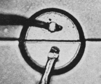
Low-drift differential amplifier uses two pairs of twin passivated
mesa transistors. Voltage gain is 40 db; drift is 10 microvolts per degree centigrade.
In the output stage of a home radio. a high voltage passivated
mesa transistor is protected by a silicon varistor.

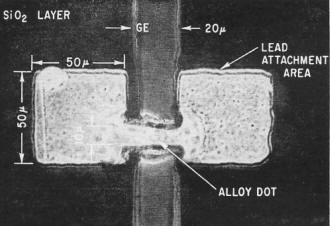
In Sony's new method of fabricating tunnel diodes, a dot of alloy
material bridges the trench between two metallized areas. The result is a more rugged
device.
Applications of Passivated Mesa Transistors
In the new Sony process, after a germanium slice has been coated with silicon
dioxide, a trench about 20 microns wide is cut in the oxide coating by photolithographic
etching. Then two regions, 50 microns by 50 microns, on each side of the trench
are metallized. An alloy dot bridges the two metallized areas over the trench, forming
a junction at the bottom of the trench and ohmic contacts to the two metallized
regions. A final etching process brings the diode to the desired characteristics
of peak current and peak-to-valley current ratio.
In a diode made this way, the etched junction is only slightly smaller than the
original junction. But the junction does not have to contribute to mechanical support;
rather, the ohmic contact region supports the junction.
Besides being stronger, the new diode has better electrical characteristics.
One which Sony produces has a cutoff frequency of 10 to 21 gigacycles, self resonant
frequency of 14 to 22 gigacycles, and a capacitance-to-peak current ratio of 0.1
to 0.25 picofarads per milliampere.
Other High-Frequency Diodes
Because of Japan's interest in and use of solid state microwave, there has been
a lot of activity in developing high-frequency diodes for communication systems.
Among the first Japanese semiconductor developments was the Kita diode or silver-bonded
diode developed at the Electrical Communications Laboratory of NTT, and now manufactured
by Nippon Electric Co.
The Kita diode has outstanding characteristics when used as a parametric amplifier,
upconverter or frequency multiplier at microwave frequencies. The reason is the
small capacitance of the depletion layer, typically less than 0.5 picofarads, and
a low series resistance, less than 10 ohms. Although the device was first developed
in 1954, its greatest applications have appeared in the past two or three years.
Now new ones are being discovered in high-speed switching, clamping and clipping.
Making the diode is relatively easy; the big difference is in the method of bonding.
In a conventional diode gold wires are used. In the Kita device, the tip of a silver
whisker, containing a small amount of gallium, contacts a bulk crystal which has
been highly doped with n type germanium or silicon. Applying a large current pulse
produces a very small area of p+ material on the crystal, completing the fabrication
of the diode.
As an indication of Japanese activity producing a variety of diodes:
• Nippon Electric Co. produces high frequency Zener diodes with low junction
capacitance.
• Fujitsu Ltd., the Nippon Electric Co., and the Mitsubishi Electric Corp.
make silicon diffused varactors for solid state microwave systems of 2, 4 and 6
Gc. The Mitsubishi MVE6006 can deliver an output of 3 watts at 4 Gc when used as
a frequency tripler. That's the highest output at this frequency of any Japanese
diode.
• The New Japan Radio Co., Ltd., Fujitsu Ltd., and the Sanyo Electric Co.
make variable-capacitance diodes with a retrograded junction, a device which is
also called a hyper-abrupt junction diode. These devices are used as a tuning element
which covers a wide frequency range and as a modulator in f-m communications systems.
• Fujitsu Ltd., has also developed a new gallium-arsenide light emitting
diode that throws a narrow beam of non coherent light through a transparent window
at the top of the mounting. It has been used in a micromanipulator which accurately
positions tools driven by a pulse motor.
Special Purpose Devices

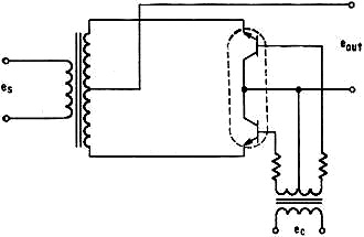
Balanced modulator has a symmetrical twin transistor (in color)
built by the Nippon Electric Co. This configuration has high conversion efficiency
and small carrier leakage because the saturation resistance and voltage are appreciably
smaller than those of diodes used in conventional modulators.
A look at some of the special purpose devices developed in Japan helps understand
both the spread of Japan's semiconductor industry and its electronics industry.
One unusual device is the V-203, a bidirectional twin transistor, built by the
Nippon Electric Co. for balanced modulators. A unique junction structure and a controlled
epitaxial technique produces symmetrical characteristics (see circuit below).
Another device is a high-speed four-layer diode developed by Mitsubishi. A two-terminal
silicon device, it has a break-over voltage of only 3 volts and a switching time
of 20 nanoseconds. Most probably application is in fast digital circuits.
And still another new device is the gate-turnoff silicon controlled rectifier
produced by Toshiba. Labeled the M8392, it has a turnoff gain of 8; that is, a gate
current of 500 milliamps can turn off a current of 4 amps.
Power Handling Devices
Although both power equipment manufacturers and transistor makers make power
handling devices - silicon rectifiers, silicon controlled rectifiers, and silicon
symmetrical switches (bidirectional four-layer diodes) - the development effort
doesn't begin to compare with that in the United States. In general, SCR's, for
example, are expensive and are not yet used widely. Until recently, Japanese SCR's
did not have the large current-carrying capacities of those available in the U.
S. and Europe.
The situation is changing and some new devices supply the strongest evidence.
A new SCR developed by Nippon Electric Co. uses a silicon slice 1% inches in diameter;
it's the biggest SCR developed in Japan. Called the V-179, it has a mean forward
current of 700 amps, repetitive peak reverse voltage of 2,350 volts, and a surge
current rating of 9,000 amps.
One not so large is the CJ-021 built by Hitachi for ac-dc conversion in a 2,200
kilowatt electric locomotive. Ratings of this SCR are: a peak reverse voltage of
1,200 volts and a mean forward current of 390 amps. Because so much of Japan's extensive
railroads net is electrified, there is likely to be an increased use of SCR's
for conversion and speed control as the manufacturing volume increases and decreases
the cost.
Hitachi has one other interesting SCR, the CR-93VE, a small high speed device.
It takes only 3 microseconds to turn on 1,000 amps, and 6 microseconds to turn off
10 amps. But it can handle 1,000 amps only for short surges.
Silicon symmetrical switches are a specialty of the Shindengen Electric Manufacturing
Co. which makes several series of them. Its KXB series contains two terminal bidirectional
switches with breakover voltages of 100 to 200 volts. The K17B-10 and K17B-20 have
a rating of 150 amps, bidirectional rms current and the K5B can handle 12 amps.
Another supplier is Hitachi, whose FR-01 is a 5-layer switch with one control
gate electrode. A control current, either positive or negative, of 100 milliamps
can fire the switch in either direction, regulating an rms current of 16 amperes.
High-Voltage Rectifiers
Still a small part of the Japanese semiconductor industry is the manufacture
of high-voltage rectifiers, capable of handling reverse voltages of 3,000 and 4,000
volts. The Hitachi HO3-DA has a peak reverse voltage of 3,000 volts and a rated
mean forward current of 470 amps. A device made by the Sanken Electric Co. has a
breakdown voltage exceeding 4,000 volts; mean forward current is 150 milliamps and
the forward voltage drop is only one volt when maximum forward current flows.
A Neat Packaging Idea
 At the Nippon Electric Co., miniature high-frequency
transistors are assembled on rolls of Kovar material to simplify manufacturing and
handling. The transistors are mounted in tiny ceramic headers called Micro Disks
which also minimize parasitic capacitances and inductance created by conventional
single-ended packages. At the Nippon Electric Co., miniature high-frequency
transistors are assembled on rolls of Kovar material to simplify manufacturing and
handling. The transistors are mounted in tiny ceramic headers called Micro Disks
which also minimize parasitic capacitances and inductance created by conventional
single-ended packages.
Assembly is simple and automated. Leads are stamped from a continuous flat strip
of Kovar. Silicon dies are mounted on the collector leads and interval leads are
attached between the base and emitter and the leads on the strip. Tiny ceramic disks,
recessed like an ashtray in the center are coated with low-melting glass, then attached
from both sides of the strip. When the assembly is heated, the glass melts and a
hermetic seal is formed. The leads are cut out from the strip and the devices separated
from each other for final testing.
Shindengen makes an avalanche rectifier diode, the S5Z-50, with a reverse surge
power rating of 2.5 kilowatts for 10 microsecond pulses. In the S5Z series, peak
reverse voltages range from 400 to 1,200 volts; mean forward current is about 20
amps.
Any survey of the Japanese semiconductor industry would not be complete without
mentioning several processing techniques which have been developed.
Many of the high voltage devices made in Japan receive a special surface treatment
called ONV, which means oxidation by nitrogen dioxide vapor. The treatment, developed
at the Electrical Communications Laboratory, consists of two processes: cleaning
the silicon surface in an atmosphere of hydrogen fluoride and nitrogen dioxide;
and oxidizing at a low temperature. Such treatment raises breakdown voltage, minimizes
leakage current and steps up the surge power rating.
Though germanium devices far outnumber silicon devices produced by Japanese semiconductor
makers, more research effort is being applied to silicon technology because it is
newer. For example, the Oki Electric Co. has perfected a simple process for depositing
polycrystal silicon.
The company has made a tiny diode with an upper ohmic contact formed by depositing
polycrystal silicon. The polycrystal material is deposited in a window cut into
oxide masking. During fabrication, it acts as an impurity source for diffusing the
p-n junction beneath it, and afterwards as a protective coating and contact to the
completed junction. This technique supplies a rigid, reliable contact that is simple;
no ball or fancy contact structure is required as it is with many kinds of silicon
diodes.
Another application of silicon polycrystal produces isolated silicon islands
in integrated circuits in a process similar to Motorola's EPIC process - but simpler.
In Motorola's process, a silicon crystal is etched to a waffle-like pattern and
then oxidized. Polycrystal is deposited over the waffle-like face; the bulk of the
single crystal material is removed by grinding and lapping until the waffle-like
projections are a group of oxide-isolated islands supported by polycrystal silicon.
In the Oki process, the starting material is a two-layer structure of thin silicon
single crystal on a polycrystal bulk. In the etch that produces the waffle-like
structure, the single crystal is cut down to the supporting polycrystal. The structure
is then oxidized and polycrystal silicon deposited just as it is in the EPIC process.
But the original poly crystal silicon is removed, leaving a group of oxide-insulated
islands supported by polycrystal silicon. What makes this process simpler is that
the polycrystal material is removed easily.
The Authors
After receiving his Ph.D. from Osaka University, Takuya Kojima (left) started
his engineering career by developing tubes for wideband amplifiers. He switched
to semiconductor devices in 1955 and now heads solid state engineering work at the
Electrical Communications Laboratory.
Ever since he graduated from the University of Tokyo in 1953, Makoto Watanabe
(right) has had an interest in semiconductors. As a staff engineer at the Electrical
Communications Laboratory, he develops high frequency germanium and silicon devices.
Posted October 23, 2023
(updated from original
post on 8/24/2018)
|


 where rbb' is the base spreading resistance,
cc is the collector capacitance and τec is the carrier
transit time between emitter and collector. The base spreading resistance and collector
capacitance degrade performance. Base spreading resistance not only decreases the
power gain and output power but also degrades the noise figure.