|
Sunshine Design Engineering Services
Joe Cahak, of Sunshine Design Engineering Services, has published yet another
paper in his series on making RF test measurements. Joe is available for
short term and long term contract work.
See list of all of Joe's articles at bottom of page.
Measuring Semiconductor Device Input Parameters with Vector Analysis
By Joe Cahak, Sunshine Design Engineering Services
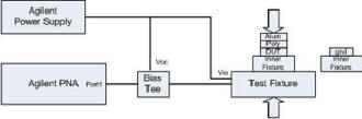
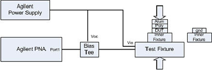
Figure 1 - Test System and Fixture
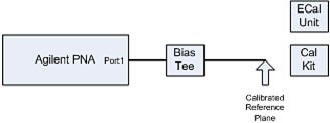
Figure 2 - Test System 1 Port Calibration
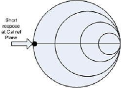
Figure 3 - Short at Cal Reference Plane
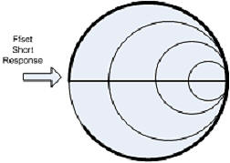
Figure 4 - Offset Short Response
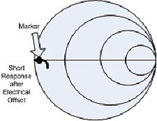
Figure 5 - Offset Short after Port Extension
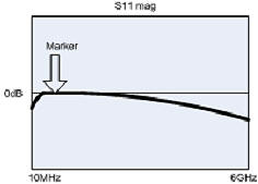
Figure 6 - Offset Short S11 Magnitude Response
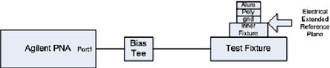
Figure 7 - Test Fixture Port Electrical Length Extension
to Short
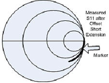
Figure 8 - Device Parameter Response after Port Extension
Offset
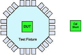
Figure 9 - Test Fixture Top View
This article will cover a recent test experience that utilized some thinking
about the test fixture, the bias requirements and the device mounting and special
calibration offsets needed to de-embed the test fixture response from the device
response within the test fixture. The device also had to have bias on several
ports simultaneously. We had to establish a "reference plane" within the fixture,
from which we can use the Vector Network Analyzer's Port Extension or Phase
Offset to dial out the distance from our 1 port calibration reference plane
to the point of short reference within the fixture. With this phase offset compensation
we can then measure the device capacitance of the part within the fixture and
the line length of the test fixture mostly worked out by the port extension.
So how did we do this? We had to start with a Vector Network Analyzer. We
also need a Bias Tee and some good RF cables. In our case, the client had a
test fixture/jig to work with that had SMA to coplanar PCB. Then a device interface
and a intermediate chip to interface to the DUT. The DUT was a CMOS RF device
and we were measuring the input capacitance of a data and clock port, while
the Vio bias line was also high.
We were able to work out a means to modify the interface chip to accommodate
the in-fixture short for the reference for the 1 port measurement of the DUT
parameter. We next worked out how to hold the parts and calibration parts in
the fixture. We inserted a coaxial bias tee and an RF coaxial cable on Port
1 of the Vector Network Analyzer. We set the VNA with a maximum range frequency
sweep with a fair number of points greater than or equal to 401 and set a 0 dBm
power level for good dynamic range for the measurement. Part of the reasoning
for the calibration setup would be if the calibration is used for analysis,
does it give high enough frequency to give small distance resolution if we had
the Time Domain option on the VNA.
For the fixture de-embedding method, we chose the first order correction
of electrical extension or port extension method. This is a simple fixture de-embed
in that it offsets the reference plane in phase only and not the amplitude loss.
The measured short response at a distance from the reference plane, or in the
fixture, can be dialed out in phase space. With this reference plane displacement
we get the phase offset of the DUT to be measured. From this phase offset remaining,
we can determine the device parameter at the frequency of the marker.
I next determined if the cal kit would be an Ecal unit or a standard coaxial
calibration kit. It does not matter which is used, either one will work. After
calibration, we have a decent measurement reference plane to start with that
is at to the fixture input. We could use raw data, but it does tend to be noisier
and bumpier due to the system non-linear frequency response of the parts in
the VNA, bias tee and RF coaxial cable. So a good 1 port calibration for a starting
point it is.
If you have a barrel SMA adapter to connect a short offset from the cal point,
you can see the effect of the offset short using the port extension. The short
response will circle the outside of the smith chart and may do more than one
loop to just a short arc around the smith chart outer boundary. The difference
is the electrical distance to the short and the arc swept out due to the frequency
response of that offset length.
So dialing the electrical length or port extension out to the short offset
will unwrap the short response on the smith chart and bring some of the frequency
response within a nice small dot as close to 1 180 as possible. Reading the electrical delay
and using the velocity factor and speed of light to compute the distance of
the wave within the fixture or Jig we are using. In our case the distance from
the SMA connector to the DUT inside the inner fixture was only about 3 inches
and was almost all coplanar line. The major discontinuity to the line characteristic
impedance is at the connector interfaces at the inner fixture and DUT within
the inner fixture. As long as the inner connect impedances are balanced with
some capacitance we can get a slow slope on the phase change with frequency
response of the fixture and DUT. So we are able to dial out the phase offset
at lower frequencies, but high frequency response may be non-linear at the higher
frequencies. So we chose 100 MHz where the S11 response was fairly stable
for a 40-800 MHz range. Within that range Cx should be relatively stable
as a function of frequency. 180 as possible. Reading the electrical delay
and using the velocity factor and speed of light to compute the distance of
the wave within the fixture or Jig we are using. In our case the distance from
the SMA connector to the DUT inside the inner fixture was only about 3 inches
and was almost all coplanar line. The major discontinuity to the line characteristic
impedance is at the connector interfaces at the inner fixture and DUT within
the inner fixture. As long as the inner connect impedances are balanced with
some capacitance we can get a slow slope on the phase change with frequency
response of the fixture and DUT. So we are able to dial out the phase offset
at lower frequencies, but high frequency response may be non-linear at the higher
frequencies. So we chose 100 MHz where the S11 response was fairly stable
for a 40-800 MHz range. Within that range Cx should be relatively stable
as a function of frequency.
Next I connect the test fixture and the inner fixture short in the outer
fixture for the port we want to measure. I next bring up the Smith Chart on
the VNA and dial the port extension until the frequency response is close to
a dot on the far left of the smith chart. This is 1180 or a short response or as close as we can
get to it. From the Cartesian plot of S11 Magnitude you can see that the short
response was very close to a real short response in the 40 to 500 MHz range
e.g. 0 dB mag and 180 degrees angle response. Make note of this as I will
refer to this again when we measure the actual part.
Next we remove the short, and insert the part. We then setup and check the
bias to the bias line and to the control line to the DUT. We double check the
voltages at the respective closest point to the DUT prior to connection of DUT.
We next bias down and insert the part and compress into the fixture. We now
get the marker value at our selected "zero" 100 MHz frequency that we choose
earlier. We have set the marker to give the Ohms & iOhms reading. The feature
of computing the device capacitance or inductance value is additionally an Agilent
PNA feature and I am sure many of the other VNA's have the same feature. Set
the marker to the Ohms & iOhms and then add the L or C readout on the marker
if necessary.
One further note on this measurement is that if the marker is placed at any
frequency within the previously mentioned frequency region where the offset
short was effectively "zeroed" out by the port extension, the reactance will
scale with the frequency such that the Cx effective is approximately the same
value for that frequency response region, where we were able to "zero" out the
short response.
For the client the measurement was a success and the results were within
acceptable limits on a typical passing value. This was a good example of one
of today's test and measurement problems with a reasonable and quick solution.
Sunshine Design Engineering Services
is located in the sunny San Vicente Valley near San Diego, CA, gateway to the mountains
and skies. Are you looking for new things to design, program or create and need
assistance? I offer design services with specialties in electronic hardware, CAD
and software engineering, and 25 years of experience with Test Engineering services
in RF/microwave, transceiver and semiconductor parametric test, test application
program development, automation programs, database programming, graphics and analysis,
and mathematical algorithms.
See also:
- RF Connectors and Cables
- Searching for the Q
- Hybrid Heaven
- Noise and Noise Measurements
- Solace in Solar
-
Measuring
Semiconductor Device Input Parameters with Vector Analysis
- Computing with Scattering Parameters
- Measurements with Scattering
Parameters
- Ponderings on Power Measurements
- Scattered Thoughts on
Scattering Parameters
Sunshine Design Engineering Services 23517 Carmena Rd
Ramona, CA 92065 760-685-1126 Featuring: Test Automation Services, RF Calculator
and S-Parameter Library (DLL & LLB)
LinkedIn:
Joe Cahak SunshineDesign@cox.net
Posted July 22, 2020
(updated from original post on 10/23/2013)
|