Module 12 - Modulation Principles
Pages i,
1-1,
1-11,
1-21,
1-31,
1-41,
1-51,
1-61,
1-71,
2-1,
2-11,
2-21,
2-31,
2-41,
2-51,
2-61,
3-1,
3-11,
3-21,
3-31, AI-1, Index, Assignment 1, 2
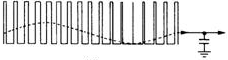
Figure 3-18K. - Gated-beam
detector waveforms. Advantages of the Gated-Beam Detector The primary advantage of the gated-beam
detector lies in its extreme simplicity. It employs only one tube, yet provides a very effective limiter with
linear detection. It requires relatively few components and is very easily adjusted. There are more than
the three types of fm demodulators presented in this chapter. However, these are representative of the types with
which you will be working. The principles involved in their operation are similar to the other types. You will now
briefly study Phase DEMODULATION which uses the same basic circuitry as fm demodulators. Q-28. What
circuit functions does the tube in a gated-beam detector serve? Q-29. What condition must exist on both
the limiter and quadrature grids for current to flow in a gated-beam detector? Q-30. Name two advantages
of the gated-beam detector. Phase DEMODULATION In phase modulation (pm) the
intelligence is contained in the amount and rate of phase shift in a carrier wave. You should recall from your
study of pm that there is an incidental shift in frequency as the phase of the carrier is shifted. Because of this
incidental frequency shift, fm demodulators, such as the Foster-Seeley discriminator and the ratio detector, can
also be used to demodulate phase-shift signals. Another circuit that may be used is the gated-beam
(quadrature) detector. Remember that the fm phase detector output was determined by the phase of the signals
present at the grids. a QUADRATURE DETECTOR for Phase DEMODULATION works in the same manner. A basic
schematic is shown in figure 3-19. The quadrature-grid signal is excited by a reference from the transmitter. This
may be a sample of the unmodulated master oscillator providing a phase reference for the detector. 3-21
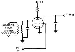
Figure 3-19. - Phase detector. The modulated waveform is applied to the limiter grid. Gating action in the tube will occur as the phase
shifts between the input waveform and the reference. The combined output current from the gated- beam tube will be
a series of current pulses. These pulses will vary in width as shown in figure 3-20. The width of these pulses
will vary in accordance with the phase difference between the carrier and the modulated wave.
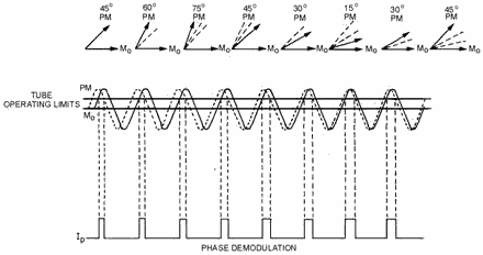
Figure 3-20. - Phase-detector waveforms. Q-31. Where is the intelligence contained in a phase-modulated signal? Q-32. Why can
phase-modulated signals be detected by fm detectors? Q-33. How is a quadrature detector changed when used
for phase demodulation? 3-22
PULSE DEMODULATION Pulse modulation is used in radar circuits as well as
communications circuits, as discussed in chapter 2. a pulse-modulated signal in radar may be detected by a
simple circuit that detects the presence of RF energy. Circuits that are capable of this were covered in this
chapter in the CW detection discussion; therefore, the information will not be repeated here. a Radar DETECTOR, in
its simplest form, must be capable of producing an output when RF energy (reflected from a target) is present at
its input. In Communications PULSE DETECTORS the modulated waveform must be restored to its original form.
In this chapter you will study three basic methods of pulse demodulation: PEAK, Low-PASS FILTER, and CONVERSION. PEAK DETECTION Peak detection uses the amplitude of a pulse-amplitude modulated (PAM)
signal or the duration of a pulse-duration modulated (PDM) signal to charge a holding capacitor and restore the
original waveform. This demodulated waveform will contain some distortion because the output wave is not a pure
sine wave. However, this distortion is not serious enough to prevent the use of peak detection.
Pulse-Amplitude Demodulation Peak detection is used to detect PAM. Figure 3-21 includes a
simplified circuit [view (A)] for this demodulator and its waveforms [views (B) and (C)]. CR1 is the input diode
which allows capacitor C1 to charge to the peak value of the PAM input pulse. Pam input pulses are shown in view
(B). CR1 is reverse biased between input pulses to isolate the detector circuit from the input. CR2 and CR3 are
biased so that they are normally nonconducting. The discharge path for the capacitor is through the resistor (R1).
These components are chosen so that their time constant is at least 10 times the interpulse period (time between
pulses). This maintains the charge on C1 between pulses by allowing only a small discharge before the next pulse
is applied. The capacitor is discharged just prior to each input pulse to allow the output voltage to follow the
peak value of the input pulses. This discharge is through CR2 and CR3. These diodes are turned on by a negative
pulse from a source that is time-synchronous with the timing-pulse train at the transmitter. Diode CR3 ensures
that the output voltage is near 0 during this discharge period. View (C) shows the output wave shape from this
circuit. The peaks of the output signal follow very closely the original modulating wave, as shown by the dotted
line. With additional filtering this stepped waveform closely approximates its original shape.
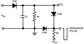
Figure 3-21A. - Peak detector. Circuit of PEAK DETECTOR. 3-23
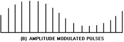
Figure 3-21B. - Peak detector. Amplitude MODULATED PULSES. 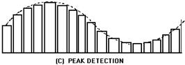
Figure 3-21C. - Peak detector. PEAK DETECTION. Pulse-Duration Modulation The peak detector circuit may also be used for PDM.
To detect PDM, you must modify view (A) of figure 3-21 so that the time constant for charging C1 through CR1 is at
least 10 times the maximum received pulse width. This may be done by adding a resistor in series with the cathode
or anode circuit of CR1. The amplitude of the voltage to which C1 charges, before being discharged by the negative
pulse, will be directly proportional to the input pulse width. a longer pulse width allows C1 to charge to a
higher potential than a short pulse. This charge is held, because of the long time constant of R1 and C1, until
the discharge pulse is applied to diodes CR2 and CR3 just prior to the next incoming pulse. These charges across
C1 result in a wave shape similar to the output shown for PAM detection in view (C) of figure 3-21.
Q-34. In its simplest form, what functions must a radar detector be capable of performing? Q-35. What
characteristic of a pulse does a peak detector sample? Q-36. What is the time constant of the resistor
and capacitor in a peak detector for PAM? Q-37. How can a peak detector for PAM be modified to detect PDM?
Low-PASS FILTER Another method of demodulating PDM is by the use of a low-pass filter. If
the voltage of a pulse waveform is averaged over both the pulse and no-pulse time, average voltage is the result.
Since the amplitude of PDM pulses is constant, average voltage is directly proportional to pulse width. The pulse
width varies with the modulation (intelligence) in PDM. Because the average value of the pulse train varies in
accordance with the modulation, the intelligence may be extracted by passing the width- modulated pulses through a
low-pass filter. The components of such a filter must be selected so that the filter passes only the desired
modulation frequencies. As the varying-width pulses are applied to the low- 3-24
pass filter, the average voltage across the filter will vary in the same way as the original
modulating voltage. This varying voltage will closely approximate the original modulating voltage.
CONVERSION
Pulse-position modulation (PPM), pulse-frequency modulation (PFM), and pulse-code modulation
(PCM) are most easily demodulated by first converting them to either PDM or PAM. After conversion these pulses are
demodulated using either peak detection or a low-pass filter. This conversion may be done in many ways, but your
study will be limited to the simpler methods. Pulse-Position Modulation
PPM can be converted to PDM by using a flip-flop circuit. (Flip flops were discussed in NEETS,
Module 9, Introduction to Wave-Generation and Wave-Shaping Circuits.) Figure 3-22 shows the waveforms for
conversion of PPM to PDM. View (A) is the pulse-modulated pulse train and view (B) is a series of reset trigger
pulses. The trigger pulses must be synchronized with the unmodulated position of the PPM pulses, but with a fixed
time delay from these pulses. As the position-modulated pulse is applied to the flip-flop, the output is driven
positive, as shown in view (C). After a period of time, the trigger pulse is again generated and drives the
flip-flop output negative and the pulse ends. Because the PPM pulses are constantly varying in position with
reference to the unmodulated pulses, the output of the flip- flop also varies in duration or width. This PDM
signal can now be applied to one of the circuits that has already been discussed for demodulation.
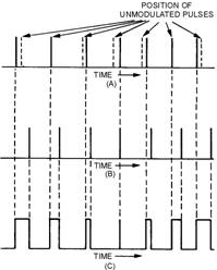
Figure 3-22. - Conversion of PPM to PDM. Pulse-frequency modulation is a variation of PPM and may be converted by the same method. 3-25
Pulse-Code Modulation Pulse-code modulation can easily be decoded, provided
the pulse-code groups have been transmitted in reverse order; that is, if the pulse with the lowest value is
transmitted first, the pulse with the highest value is transmitted last. a circuit that will provide a constant
value of current without regard to its load is known as a current source. a current source is used to apply the
PCM pulses to an RC circuit, such as that shown in figure 3-23, view (A). The current source must be capable of
supplying a linear charge to C1 that will increase each time a pulse is applied if C1 is not allowed to discharge
between pulses. In other words, if C1 charges to 16 volts during the period of one pulse, then each additional
pulse increases the charge by 16 volts. Thus, the cumulative value increases by 16 volts for each received pulse.
This does not provide a usable output unless a resistor is chosen that allows C1 to discharge to one-half its
value between pulses. If only one pulse is received at T1, C1 charges to 16 volts and then begins to discharge. At
T2 the charge has decayed to 8 volts and continues to decay unless another pulse is received. At T3 it has a
4-volt charge and at T4 it only has a 2-volt charge. At the sampling time, a 1-volt charge remains; this charge
corresponds to the binary-weighted pulse train of 0001. Now we will apply a PCM signal which corresponds to the
binary-coded equivalent of 7 volts (0111) in figure 3-23, view (A). View (B) is the pulse code that is received.
Remember that the pulses are transmitted in reverse order. View (C) is the response curve of the circuit. At T1
the pulse corresponding to the least significant digit is applied and C1 charges to 16 volts. C1 discharges
between pulses until it reaches 8 volts at T2. At T2 another pulse charges it to 24 volts. At T3, C1 has
discharged through R1 to a value of 12 volts. The pulse at T3 increases the charge on C1 by 16 volts to a total
charge of 28 volts. At T4, C1 has discharged to one-half its value and is at 14 volts. No pulse is present at T4
so C1 will not receive an additional charge. C1 continues to discharge until T5 when it has reached 7 volts and is
sampled to provide a PAM pulse which can be peak detected. This sampled output corresponds to the original
sampling of the analog voltage in the modulation. 3-26
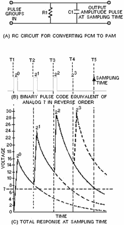
Figure 3-23. - PCM conversion. When the PCM demodulator recognizes the presence or absence of pulses in each position, it reproduces
the correct standard amplitude represented by the pulse code group. For this reason, noise introduces no error if
the largest peaks of noise are not mistaken for pulses. The PCM signal can be retransmitted as many times as
desired without the introduction of additional noise effects so long as the signal-to-noise ratio is maintained at
a level where noise pulses are not mistaken for a signal pulse. This is not the only method for demodulating PCM,
but it is one of the simplest. This completes your study of demodulation. You should remember that this module
has been a basic introduction to the principles of modulation and demodulation. With the advent of solid-state
electronics, integrated circuits have replaced discrete components. Although you cannot trace the signal flow
through 3-27
these circuits, the end result of the electronic action within the integrated circuit is the same as
it would be with discrete components. Q-38. How does a low-pass filter detect PDM? Q-39. How
is conversion used in pulse demodulation? Q-40. What is the discharge rate for the capacitor in a PCM
converter? Summary Now that you have completed this chapter, a short
review of what you have learned is in order. The following summary will refresh your memory of demodulation, its
basic principles, and typical circuitry required to accomplish this task. DEMODULATION,
also called
DETECTION, is the process of re-creating original modulating frequencies (intelligence) from
radio frequencies. The DEModulator, or DETECTOR, is the circuit in which
the original modulating frequencies are restored. A CW DEModulator is a circuit that is
capable of detecting the presence of RF energy.
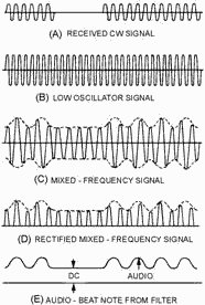
HETERODYNE DETECTION uses a locally generated frequency to beat with the CW carrier frequency
to provide an audio output. 3-28
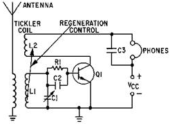
The Regenerative DETECTOR produces its own oscillations, heterodynes them with an
incoming signal, and detects them.
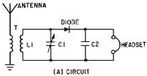
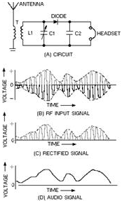
The Series- (Voltage-) DIODE DETECTOR has a rectifier diode that is in series with the
input voltage and the load impedance. 3-29
Shunt- (CURRENT-) DIODE DETECTOR is characterized by a rectifier diode in parallel with
the input and load impedance.
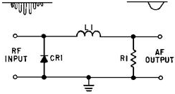
The Common-Emitter DETECTOR is usually used in receivers to supply a detected and
amplified output. 3-30
| - |
Matter, Energy,
and Direct Current |
| - |
Alternating Current and Transformers |
| - |
Circuit Protection, Control, and Measurement |
| - |
Electrical Conductors, Wiring Techniques,
and Schematic Reading |
| - |
Generators and Motors |
| - |
Electronic Emission, Tubes, and Power Supplies |
| - |
Solid-State Devices and Power Supplies |
| - |
Amplifiers |
| - |
Wave-Generation and Wave-Shaping Circuits |
| - |
Wave Propagation, Transmission Lines, and
Antennas |
| - |
Microwave Principles |
| - |
Modulation Principles |
| - |
Introduction to Number Systems and Logic Circuits |
| - |
- Introduction to Microelectronics |
| - |
Principles of Synchros, Servos, and Gyros |
| - |
Introduction to Test Equipment |
| - |
Radio-Frequency Communications Principles |
| - |
Radar Principles |
| - |
The Technician's Handbook, Master Glossary |
| - |
Test Methods and Practices |
| - |
Introduction to Digital Computers |
| - |
Magnetic Recording |
| - |
Introduction to Fiber Optics |
| Note: Navy Electricity and Electronics Training
Series (NEETS) content is U.S. Navy property in the public domain. |
|