Module 8 - Introduction to Amplifiers
Pages i,
1-1,
1-11,
1-21,
1-31,
2-1,
2-11,
2-21,
2-31,
3-1,
3-11,
3-21,
3-31,
3-41,
3-51,
3-61,
AI-1,
Index
| - |
Matter, Energy,
and Direct Current |
| - |
Alternating Current and Transformers |
| - |
Circuit Protection, Control, and Measurement |
| - |
Electrical Conductors, Wiring Techniques,
and Schematic Reading |
| - |
Generators and Motors |
| - |
Electronic Emission, Tubes, and Power Supplies |
| - |
Solid-State Devices and Power Supplies |
| - |
Amplifiers |
| - |
Wave-Generation and Wave-Shaping Circuits |
| - |
Wave Propagation, Transmission Lines, and
Antennas |
| - |
Microwave Principles |
| - |
Modulation Principles |
| - |
Introduction to Number Systems and Logic Circuits |
| - |
- Introduction to Microelectronics |
| - |
Principles of Synchros, Servos, and Gyros |
| - |
Introduction to Test Equipment |
| - |
Radio-Frequency Communications Principles |
| - |
Radar Principles |
| - |
The Technician's Handbook, Master Glossary |
| - |
Test Methods and Practices |
| - |
Introduction to Digital Computers |
| - |
Magnetic Recording |
| - |
Introduction to Fiber Optics |
| Note: Navy Electricity and Electronics Training
Series (NEETS) content is U.S. Navy property in the public domain. |
...Pages
1-11 to 1-20
The feedback network in this amplifier is made up of R2 and C2. The value of
C2 should be large so that the capacitive reactance (X C) will be low and the capacitor
will couple the signal easily. (This is also the case with the input and output
coupling capacitors C1 and C3.) The resistive value of R2 should be large to limit
the amount of feedback signal and to ensure that the majority of the output signal
goes on to the next stage through C3.

Figure 1-18 - Positive feedback in a transistor amplifier.

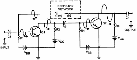
Figure 1-19 - Positive feedback in two stages of transistor amplification.
A more common configuration for transistor amplifiers is the common-emitter configuration.
Positive feedback is a little more difficult with this configuration because the
input and output signals are 180º out of phase. Positive feedback can be accomplished
by feeding a portion of the output signal of the second stage back to the input
of the first stage. This arrangement is shown in figure 1-19.
The figure shows that each stage of amplification has a 180º phase shift. This
means that the output signal of Q2 will be in phase with the input signal to Q1.
a portion of the output signal of Q2 is coupled back to the input of Q1 through
the feedback network of C3 and R3. R3 should have a large resistance to limit the
amount of signal through the feedback network. C3 should have a large capacitance
so the capacitive reactance is low and the capacitor will couple the signal easily.
Sometimes positive feedback is used to eliminate the effects of negative feedback
that are caused by circuit components. One way in which a circuit component can
cause negative feedback is shown in figure 1-20.
In view (A) a common-emitter transistor amplifier is shown. An emitter resistor
(R2) has been placed in this circuit to provide proper biasing and temperature stability.
An undesired effect of this resistor is the development of a signal at the emitter
in phase with the input signal on the base. This signal is caused by the changing
current through the emitter resistor (R2) as the current through the transistor
changes. You might think that this signal on the emitter is a form of positive feedback
since it is in phase with the input signal. But the emitter signal is really negative
feedback. Current through the transistor is controlled by the base-to-emitter bias.
If both the base and emitter become more positive by the same amount at the same
time, current will not increase. It is the difference between the base and emitter
voltages that controls the current flow through the transistor.
To eliminate this negative feedback caused by the emitter resistor, some way
must be found to remove the signal from the emitter. If the signal could be coupled
to ground (decoupled) the emitter of the transistor would be unaffected. That is
exactly what is done. a Decoupling Capacitor (C3 in view B) is placed between the
emitter of Q1 and ground (across the emitter resistor). This capacitor should have
a high capacitance so that it will pass the signal to ground easily. The decoupling
capacitor (C3) should have the same qualities as the coupling capacitors (C1 and
C2) of the circuit. Decoupling capacitors are also called bypass capacitors.

Figure 1-20A. - Decoupling (bypass) capacitor in a transistor
amplifier.
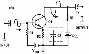
Figure 1-20B - Decoupling (bypass) capacitor in a transistor
amplifier.
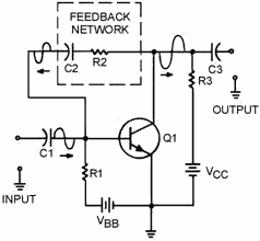
Figure 1-21 - Negative feedback in a transistor amplifier.
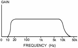
Figure 1-22 - Ideal frequency response curve for an audio amplifier.
Regardless of the method used to provide positive feedback in a circuit, the
purpose is to increase the output signal amplitude.
Negative Feedback
Negative feedback is accomplished by adding part of the output signal out of
phase with the input signal. You have seen that an emitter resistor in a common-emitter
transistor amplifier will develop a negative feedback signal. Other methods of providing
negative feedback are similar to those methods used to provide positive feedback.
The phase relationship of the feedback signal and the input signal is the only difference.
Figure 1-21 shows negative feedback in a common-emitter transistor amplifier.
The feedback network of C2 and R2 couples part of the output signal of Q1 back to
the input. Since the output signal is 180º out of phase with the input signal, this
causes negative feedback.
Negative feedback is used to improve fidelity of an amplifier by limiting the
input signal. Negative feedback can also be used to increase the frequency response
of an amplifier. The gain of an amplifier decreases when the limit of its frequency
response is reached. When negative feedback is used, the feedback signal decreases
as the output signal decreases. At the limits of frequency response of the amplifier
the smaller feedback signal means that the effective gain (gain with feedback) is
increased. This will improve the frequency response of the amplifier.
Q-23. What is feedback?
Q-24. What are the two types of feedback?
Q-25. What type feedback provides increased amplitude output signals?
Q-26. What type feedback provides the best fidelity?
Q-27. If the feedback signal is out of phase with the input signal, what type
feedback is provided?
Q-28. What type feedback is provided by an unbypassed emitter resistor in a common-emitter
transistor amplifier?
Audio Amplifiers
An audio amplifier has been described as an amplifier with a frequency response
from 15 Hz to 20 kHz. The frequency response of an amplifier can be shown graphically
with a frequency response curve. Figure 1-22 is the ideal frequency response curve
for an audio amplifier. This curve is practically "flat" from 15 Hz to 20 kHz. This
means that the gain of the amplifier is equal between 15 Hz and 20 kHz. Above 20
kHz or below 15 Hz the gain decreases or "drops off" quite rapidly. The frequency
response of an amplifier is determined by the components in the circuit.
The difference between an audio amplifier and other amplifiers is the frequency
response of the amplifier. In the next chapter of this module you will be shown
the techniques and components used to change and extend the frequency response of
an amplifier.
The transistor itself will respond quite well to the audio frequency range. No
special components are needed to extend or modify the frequency response.
You have already been shown the purpose of all the components in a transistor
audio amplifier. In this portion of the chapter, schematic diagrams of several audio
amplifiers will be shown and the functions of each of the components will be discussed.
Single-Stage Audio Amplifiers
The first single-stage audio amplifier is shown in figure 1-23. This circuit
is a class A, common-emitter, RC-coupled, transistor, audio amplifier. C1 is a coupling
capacitor that couples the input signal to the base of Q1. R1 is used to develop
the input signal and provide bias for the base of Q1. R2 is used to bias the emitter
and provide temperature stability for Q1. C2 is used to provide decoupling (positive
feedback) of the signal that would be developed by R2. R3 is the collector load
for Q1 and develops the output signal. C3 is a coupling capacitor that couples the
output signal to the next stage. VCC represents the collector-supply voltage. Since
the transistor is a common-emitter configuration, it provides voltage amplification.
The input and output signals are 180º out of phase. The input and output impedance
are both medium.
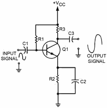
Figure 1-23 - Transistor audio amplifier.
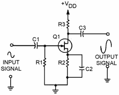
Figure 1-24 - FET audio amplifier.
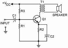
Figure 1-25 - Single-stage audio amplifier.
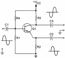
Figure 1-27 - Single-stage transistor phase splitter.
There is nothing new presented in this circuit. You should understand all of
the functions of the components in this circuit. If you do not, look back at the
various sections presented earlier in this chapter.
The second single-stage audio amplifier is shown in figure 1-24. This circuit
is a class A, common-source, RC-coupled, FET, audio amplifier. C1 is a coupling
capacitor which couples the input signal to the gate of Q1. R1 is used to develop
the input signal for the gate of Q1. R2 is used to bias the source of Q1. C2 is used to decouple the signal developed by R2 (and keep it from affecting the source
of Q1). R3 is the drain load for Q1 and develops the output signal. C3 couples the
output signal to the next stage. VDD is the supply voltage for the drain of Q1.
Since this is a common-source configuration, the input and output signals are 180º
out of phase.
If you do not remember how a FET works, refer to NEETS Module 7 Introduction
to Solid-State Devices and Power Supplies.
The third single-stage audio amplifier is shown in figure 1-25. This is a class
A, common-emitter, transformer-coupled, transistor, audio amplifier. The output
device (speaker) is shown connected to the secondary winding of the transformer.
C1 is a coupling capacitor which couples the input signal to the base of Q1. R1
develops the input signal. R2 is used to bias the emitter of Q1 and provides temperature
stability. C2 is a decoupling capacitor for R2. R3 is used to bias the base of Q1.
The primary of T1 is the collector load for Q1 and develops the output signal. T1
couples the output signal to the speaker and provides impedance matching between
the output impedance of the transistor (medium) and the impedance of the speaker
(low).
Phase Splitters
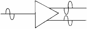
Figure 1-26 - Block diagram of a phase splitter.
Sometimes it is necessary to provide two signals that are equal in amplitude
but 180º out of phase with each other. (You will see one use of these two signals
a little later in this chapter.) The two signals can be provided from a single input
signal by the use of a Phase Splitter. a phase splitter is a device that produces
two signals that differ in phase from each other from a single input signal. Figure
1-26 is a block diagram of a phase splitter.
One way in which a phase splitter can be made is to use a center-tapped transformer.
As you may remember from your study of transformers, when the transformer secondary
winding is center-tapped, two equal amplitude signals are produced. These signals
will be 180º out of phase with each other. So a transformer with a center-tapped
secondary fulfills the definition of a phase splitter.
A transistor amplifier can be configured to act as a phase splitter. One method
of doing this is shown in figure 1-27.
C1 is the input signal coupling capacitor and couples the input signal to the
base of Q1. R1 develops the input signal. R2 and R3 develop the output signals.
R2 and R3 are equal resistances to provide equal amplitude output signals. C2 and
C3 couple the output signals to the next stage. R4 is used to provide proper bias
for the base of Q1.
This phase splitter is actually a single transistor combining the qualities of
the common-emitter and common-collector configurations. The output signals are equal
in amplitude of the input signal, but are 180º out of phase from each other.
If the output signals must be larger in amplitude than the input signal, a circuit
such as that shown in figure 1-28 will be used.
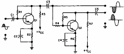
Figure 1-28 shows a two-stage phase splitter. C1 couples the input signal to
the base of Q1. R1 develops the input signal and provides bias for the base of Q1.
R2 provides bias and temperature stability for Q1. C2 decouples signals from the
emitter of Q1. R3 develops the output signal of Q1. Since Q1 is configured as a
common-emitter amplifier, the output signal of Q1 is 180º out of phase with the
input signal and larger in amplitude. C3 couples this output signal to the next
stage through R4. R4 allows only a small portion of this output signal to be applied
to the base of Q2. R5 develops the input signal and provides bias for the base of
Q2. R6 is used for bias and temperature stability for Q2. C4 decouples signals from
the emitter of Q2. R7 develops the output signal from Q2. Q2 is configured as a
common-emitter amplifier, so the output signal is 180º out of phase with the input
signal to Q2 (output signal from Q1). The input signal to Q2 is 180º out of phase
with the original input signal, so the output from Q2 is in phase with the original
input signal. C5 couples this output signal to the next stage. So the circuitry
shown provides two output signals that are 180º out of phase with each other. The
output signals are equal in amplitude with each other but larger than the input
signal.
Q-29. What is a phase splitter?
Push-Pull Amplifiers

Figure 1-28 - Two-stage transistor phase splitter.
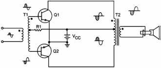
Figure 1-29 - Class A transistor push-pull amplifier.
One use of phase splitters is to provide input signals to a single-stage amplifier
that uses two transistors. These transistors are configured in such a way that the
two outputs, 180º out of phase with each other, combine. This allows more gain than
one transistor could supply by itself. This "push-pull" amplifier is used where
high power output and good fidelity are needed: receiver output stages, public address
amplifiers, and AM modulators, for example.
The circuit shown in figure 1-29 is a class a transistor push-pull amplifier,
but class AB or class B operations can be used. Class operations were discussed
in an earlier topic. The phase splitter for this amplifier is the transformer T1,
although one of the phase splitters shown earlier in this topic could be used. R1
provides the proper bias for Q1 and Q2. The tapped secondary of T1 develops the
two input signals for the bases of Q1 and Q2. Half of the original input signal
will be amplified by Q-1, the other half by Q-2. T2 combines (couples) the amplified
output signal to the speaker and provides impedance matching.
Q-30. What is one use for a splitter?
Q-31. What is a common use for a push-pull amplifier?
Q-32. What is the advantage of a push-pull amplifier?
Q-33. What class of operation can be used with a push-pull amplifier to provide
good fidelity output signals?
Summary
This chapter has presented some general information that applies to all amplifiers,
as well as some specific information about transistor and audio amplifiers. All
of this information will be useful to you in the next chapter of this module and
in your future studies of electronics.
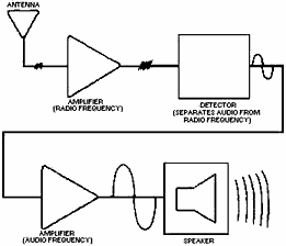
RF and audio amplifiers.
An Amplifier is a device that enables an input signal to control
an output signal. The output signal will have some (or all) of the characteristics
of the input signal but will generally be larger than the input signal in terms
of voltage, current, or power. a basic line diagram of an amplifier is shown below.
Amplifiers are classified by Function and Frequency Response. Function refers
to an amplifier being a Voltage Amplifier or a Power Amplifier. Voltage amplifiers
provide voltage amplification and power amplifiers provide power amplification.
The frequency response of an amplifier can be described by classifying the amplifier
as an Audio Amplifier, RF Amplifier, or Video (Wide-Band) Amplifier. Audio amplifiers
have frequency response in the range of 15 Hz to 20 kHz. An RF amplifier has a frequency
response in the range of 10 kHz to 100,000 MHz. a video (wide-band) amplifier has
a frequency response of 10 Hz to 6 MHz.
...Pages 1-31 to 1-40
|