Module 8 - Introduction to Amplifiers
Pages i,
1-1,
1-11,
1-21,
1-31,
2-1,
2-11,
2-21,
2-31,
3-1,
3-11,
3-21,
3-31,
3-41,
3-51,
3-61,
AI-1,
Index
| - |
Matter, Energy,
and Direct Current |
| - |
Alternating Current and Transformers |
| - |
Circuit Protection, Control, and Measurement |
| - |
Electrical Conductors, Wiring Techniques,
and Schematic Reading |
| - |
Generators and Motors |
| - |
Electronic Emission, Tubes, and Power Supplies |
| - |
Solid-State Devices and Power Supplies |
| - |
Amplifiers |
| - |
Wave-Generation and Wave-Shaping Circuits |
| - |
Wave Propagation, Transmission Lines, and
Antennas |
| - |
Microwave Principles |
| - |
Modulation Principles |
| - |
Introduction to Number Systems and Logic Circuits |
| - |
- Introduction to Microelectronics |
| - |
Principles of Synchros, Servos, and Gyros |
| - |
Introduction to Test Equipment |
| - |
Radio-Frequency Communications Principles |
| - |
Radar Principles |
| - |
The Technician's Handbook, Master Glossary |
| - |
Test Methods and Practices |
| - |
Introduction to Digital Computers |
| - |
Magnetic Recording |
| - |
Introduction to Fiber Optics |
| Note: Navy Electricity and Electronics Training
Series (NEETS) content is U.S. Navy property in the public domain. |
happens when you select a channel on your television
set or tune to a station on your radio. To accomplish this "tuning," you need only
change the value of inductance or capacitance in the parallel LC circuits (tuned
circuits).
In most cases, the capacitance is changed by the use of variable capacitors.
The capacitors in the input and output portions of all the RF amplifier stages are
ganged together in order that they can all be changed at one time with a single
device, such as the tuning dial on a radio. (This technique will be shown on a schematic
a little later in this chapter.)
Q-20. If the input-signal-developing impedance of an amplifier is increased,
what is the effect on the gain?
Q-21. If the output impedance of an amplifier circuit is decreased, what
is the effect on the gain?
Q-22. What is the purpose of a frequency-determining network in an RF amplifier?
Q-23. Can a parallel LC circuit be used as the frequency-determining network
for an RF amplifier?
Q-24. How can the frequency be changed in the frequency-determining network?
RF Amplifier Coupling
Figure 2-14 and the other circuits you have been shown use capacitors to couple
the signal in to and out of the circuit (C1 and C4 in figure 2-14). As you remember
from chapter 1, there are also other methods of coupling signals from one stage
to another. Transformer coupling is the most common method used to couple RF amplifiers.
Transformer coupling has many advantages over RC coupling for rf
amplifiers; for example, transformer coupling uses fewer components than capacitive
coupling. It can also provide a means of increasing the gain of the stage by using
a step-up transformer for voltage gain. If a
current gain is required, a step-down transformer can be used.
You should also remember that the primary and secondary windings of a transformer
are inductors. With these factors in mind, an RF amplifier could be constructed
like the one shown in figure 2-15.
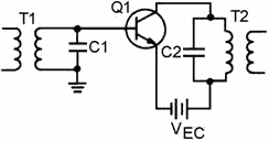
Figure 2-15. - Transformer-coupled RF amplifier.
In this circuit, the secondary of T1 and capacitor C1 form a tuned circuit which
is the input-signal- developing impedance. The primary of T2 and capacitor C2 are
a tuned circuit which acts as the output impedance of Q1. (Both T1 and T2 must be
RF transformers in order to operate at RF frequencies.)
The input signal applied to the primary of T1 could come from the previous stage
or from some input device, such as a receiving antenna. In either case, the input
device would have a capacitor connected
2-21
across a coil to form a tuned circuit. In the same way, the secondary of T2 represents
the output of this circuit. a capacitor connected across the secondary of T2 would
form a parallel LC network. This network could act as the input-signal-developing
impedance for the next stage, or the network could represent some type of output
device, such as a transmitting antenna.
The tuned circuits formed by the transformer and capacitors may not have the
bandwidth required for the amplifier. In other words, the bandwidth of the tuned
circuit may be too "narrow" for the requirements of the amplifier. (For example,
the RF amplifiers used in television receivers usually require a bandwidth of 6
MHz.)
One way of "broadening" the bandpass of a tuned circuit is to use a swamping
resistor. This is similar to the use of the swamping resistor that was shown with
the series peaking coil in a video amplifier. A swamping resistor connected in parallel
with the tuned circuit will cause a much broader bandpass. (This technique and the
theory behind it are discussed in more detail in NEETS, Module 9.)
Another technique used to broaden the bandpass involves the amount of coupling
in the transformers. For transformers, the term "coupling" refers to the amount
of energy transferred from the primary to the secondary of the transformer. This
depends upon the number of flux lines from the primary that intersect, or cut, the
secondary. When more flux lines cut the secondary, more energy is transferred.
Coupling is mainly a function of the space between the primary and secondary
windings. a transformer can be loosely coupled (having little transfer of energy),
optimumly coupled (just the right amount of energy transferred), or overcoupled
(to the point that the flux lines of primary and secondary windings interfere with
each other).
Figure 2-16, (view A) (view B) (view C), shows the effect of coupling on frequency
response when parallel LC circuits are made from the primary and secondary windings
of transformers.
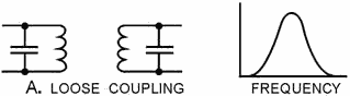
Figure 2-16A. - Effect of coupling on frequency response. LOOSE Coupling
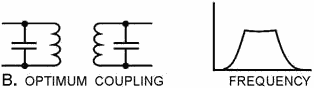
Figure 2-16B. - Effect of coupling on frequency response. OPTIMUM Coupling
2-22
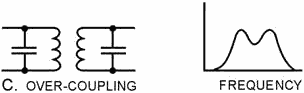
Figure 2-16C. - Effect of coupling on frequency response. OVER-Coupling
In view (A) the transformer is loosely coupled; the frequency response curve
shows a narrow bandwidth. In view (B) the transformer has optimum coupling; the
bandwidth is wider and the curve is relatively flat. In view (C) the transformer
is overcoupled; the frequency response curve shows a broad bandpass, but the curve
"dips" in the middle showing that these frequencies are not developed as well as
others in the bandwidth.
Optimum coupling will usually provide the necessary bandpass for the frequency-determining
network (and therefore the RF amplifier). For some uses, such as RF amplifiers in
a television receiver, the bandpass available from optimum coupling is not wide
enough. In these cases, a swamping resistor (as mentioned earlier) will be used
with the optimum coupling to broaden the bandpass.
Compensation of RF Amplifiers
Now you have been shown the way in which an RF amplifier is configured to amplify
a band of frequencies and the way in which an RF amplifier can be "tuned" for a
particular band of frequencies. You have also seen some ways in which the bandpass
of an RF amplifier can be adjusted. However, the frequencies at which RF amplifiers
operate are so high that certain problems exist.
One of these problems is the losses that can occur in a transformer at these
high frequencies. Another problem is with interelectrode capacitance in the transistor.
The process of overcoming these problems is known as Compensation.
Transformers in RF Amplifiers
As you recall from NEETS, Module 1, the losses in a transformer are classified
as copper loss, eddy-current loss, and hysteresis loss. Copper loss is not affected
by frequency, as it depends upon the resistance of the winding and the current through
the winding. Similarly, eddy-current loss is mostly a function of induced voltage
rather than the frequency of that voltage. Hysteresis loss, however, increases as
frequency increases.
Hysteresis loss is caused by the realignment of the magnetic domains in the core
of the transformer each time the polarity of the magnetic field changes. As the
frequency of the a.c. increases, the number of shifts in the magnetic field also
increases (two shifts for each cycle of a.c.); therefore, the "molecular friction"
increases and the hysteresis loss is greater. This increase in hysteresis loss causes
the efficiency of the transformer (and therefore the amplifier) to decrease. The
energy that goes into hysteresis loss is taken away from energy that could go into
the signal.
RF Transformers, specially designed for use with RF, are used to correct the
problem of excessive hysteresis loss in the transformer of an RF amplifier. The
windings of RF transformers are wound onto a tube of nonmagnetic material and the
core is either powdered iron or air. These types of cores also reduce
2-23
Neutralization of RF Amplifiers
The problem of interelectrode capacitance in the transistor of an RF amplifier
is solved by Neutralization. Neutralization is the process of counteracting or "neutralizing"
the effects of interelectrode capacitance.
Figure 2-17 shows the effect of the base-to-collector interelectrode capacitance
in an RF amplifier. The "phantom" capacitor (CBC) represents the interelectrode
capacitance between the base and the collector of Q1. This is the interelectrode
capacitance that has the most effect in an RF amplifier. As you can see, CBC
causes a degenerative (negative) feedback which decreases the gain of the amplifier.
(There are some special cases in which CBC can cause regenerative (positive)
feedback. In this case, the technique described below will provide negative feedback
which will accomplish the neutralization of the amplifier.)

Figure 2-17. - Interelectrode capacitance in an RF amplifier.
As you may recall, unwanted degenerative feedback can be counteracted (neutralized)
by using positive feedback. This is exactly what is done to neutralize an RF amplifier.
Positive feedback is accomplished by the use of a feedback capacitor. This capacitor
must feed back a signal that is in phase with the signal on the base of Q1. One
method of doing this is shown in figure
2-18.
2-24
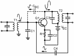
Figure 2-18. - Neutralized RF amplifier.
In figure 2-18, a feedback capacitor (C4) has been added to neutralize the amplifier.
This solves the problem of unwanted degenerative feedback. Except for capacitor
C4, this circuit is identical to the circuit shown in figure 2-17. (When CBC
causes regenerative feedback, C4 will still neutralize the amplifier. This is true
because C4 always provides a feedback signal which is 180 degrees out of phase with
the feedback signal caused by CBC.)
Q-25. What is the most common form of coupling for an RF amplifier?
Q-26. What are two advantages of this type of coupling?
Q-27. If current gain is required from an RF amplifier, what type of component
should be used as an output coupling element?
Q-28. What problem is caused in an RF amplifier by a loosely coupled transformer?
Q-29. How is this problem corrected?
Q-30. What problem is caused by overcoupling in a transformer?
Q-31. What method provides the widest bandpass?
Q-32. What two methods are used to compensate for the problems that cause
low gain in an RF amplifier?
Q-33. What type of feedback is usually caused by the base-to-collector
interelectrode capacitance?
Q-34. How is this compensated for?
Typical RF Amplifier Circuits
As a technician, you will see many different RF amplifiers in many different
pieces of equipment. The particular circuit configuration used for an RF amplifier
will depend upon how that amplifier is used. In the final part of this chapter,
you will be shown some typical RF amplifier circuits.
2-25
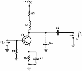
Figure 2-19 is the schematic diagram of a typical RF amplifier that is used in
an AM radio receiver. In figure 2-19, the input circuit is the antenna of the radio
(L1-a coil) which forms part of an LC circuit which is tuned to the desired station
by variable capacitor C1. L1 is wound on the same core as L2, which couples the
input signal through C2 to the transistor (Q1). R1 is used to provide proper bias
to Q1 from the base power supply (VBB). R2 provides proper bias to the emitter of
Q1, and C3 is used to bypass R2. The primary of T1 and capacitor C4 form a parallel
LC circuit which acts as the load for Q1. This LC circuit is tuned by C4, which
is ganged to C1 allowing the antenna and the LC circuit to be tuned together. The
primary of T1 is center-tapped to provide proper impedance matching with Q1.
Figure 2-19. - Typical AM radio RF amplifier.
You may notice that no neutralization is shown in this circuit. This circuit
is designed for the AM broadcast band (535 kHz - 1605 kHz).
At these relatively low RF frequencies the degenerative feedback caused by base-to-collector
interelectrode capacitance is minor and, therefore, the amplifier does not need
neutralization.
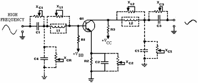
Figure 2-20 is a typical RF amplifier used in a vhf television receiver. The
input-signal-developing circuit for this amplifier is made up of L1, C1, and C2.
The inductor tunes the input-signal-developing circuit for the proper TV channel.
(L1 can be switched out of the circuit and another inductor switched in to the circuit
by the channel selector.) R1 provides proper bias to Q1 from the base supply voltage
(VBB). Q1 is the transistor. Notice that the case of Q1 (the dotted circle around
the transistor symbol) is shown to be grounded. The case must be grounded because
of the high frequencies (54 MHz - 217 MHz) used by the circuit. R2 provides proper
bias from the emitter of Q1, and C3 is used to bypass R2. C5 and L2 are a parallel
LC circuit which acts as the load for Q1. The LC circuit is tuned by L2 which is
switched in to and out of the LC circuit by the channel selector. L3 and C6 are
a parallel LC circuit which develops the signal for the next stage. The parallel
LC circuit is tuned by L3 which is switched in to and out of the LC circuit by the
channel selector along with L1 and L2. (L1, L2, and L3 are actually part of a bank
of inductors. L1, L2, and L3 are in the circuit when the channel selector is on
channel 2. For other channels, another group of three inductors would be used in
the circuit.) R3 develops a signal which is fed through C4 to provide neutralization.
This counteracts the effects of the interelectrode capacitance from the base to
the collector of Q1. C7 is used to isolate the RF signal from the collector power
supply (VCC).
2-26
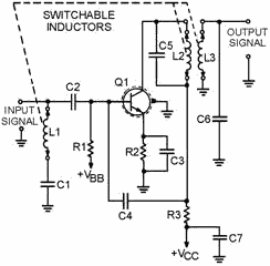
Figure 2-20. - Typical VHF television RF amplifier.
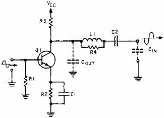
The following questions refer to figure 2-21.
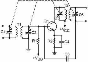
Figure 2-21. - Typical RF amplifier.
Q-35. What components form the input-signal-developing impedance
for the amplifier?
Q-36. What is the purpose of R1?
2-27
Q-37. What is the purpose of R2?
Q-38. If C4 were removed from the circuit, what would happen to the
output of the amplifier?
Q-39. What components form the load for Q1?
Q-40. How many tuned parallel LC circuits are shown in this schematic?
Q-41. What do the dotted lines connecting C1, C2, C5, and C6
indicate?
Q-42. What is the purpose of C3?
Summary
This chapter has presented information on video and RF amplifiers. The information
that follows summarizes the important points of this chapter.
A Frequency-Response Curve will enable you to determine the
Bandwidth and the Upper and LowER Frequency LIMITS of an amplifier.
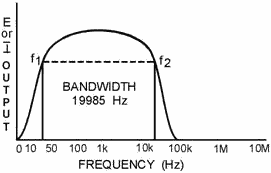
The Bandwidth of an amplifier is determined by the formula:
2-28
The Upper-Frequency Response of an amplifier is limited by the
inductance and capacitance of the circuit.
The Interelectrode Capacitance of a transistor causes Degenerative
Feedback at high frequencies.
Video Amplifiers must have a frequency response of 10 hertz
to 6 megahertz (10 Hz - 6 MHz). To provide this frequency response, both high- and
low-frequency compensation must be used.
Peaking Coils are used in video amplifiers to overcome the high-frequency
limitations caused by the capacitance of the circuit.
2-29
Series Peaking is accomplished by a peaking coil in series with
the output-signal path.
Shunt Peaking is accomplished by a peaking coil in parallel
(shunt) with the output-signal path.
2-30
|