Electronics & High Technology Components
- See Full List of AI Topics -
 The
Yagi–Uda antenna,
often referred to simply as the Yagi antenna, was developed in the late 1920s by
Japanese engineers Hidetsugu Yagi and Shintaro Uda at Tohoku University in Sendai,
Japan. The primary motivation for their work was to design a highly directional
antenna capable of efficiently transmitting and receiving radio waves over specific
frequencies. This need arose as radio communications technology was rapidly advancing,
with an emphasis on improving signal strength and selectivity for applications in
research and burgeoning communication systems. Mssrs. Yagi and Uda sought to
enhance the performance of basic dipole antennas by creating an array that exhibited
improved directivity and gain. The
Yagi–Uda antenna,
often referred to simply as the Yagi antenna, was developed in the late 1920s by
Japanese engineers Hidetsugu Yagi and Shintaro Uda at Tohoku University in Sendai,
Japan. The primary motivation for their work was to design a highly directional
antenna capable of efficiently transmitting and receiving radio waves over specific
frequencies. This need arose as radio communications technology was rapidly advancing,
with an emphasis on improving signal strength and selectivity for applications in
research and burgeoning communication systems. Mssrs. Yagi and Uda sought to
enhance the performance of basic dipole antennas by creating an array that exhibited
improved directivity and gain.
The design was first described by Uda in 1926 in Japanese and was later popularized
by Yagi, who presented the concept internationally in 1928. This antenna consists
of a driven element, which is typically a half-wave dipole, a reflector element
placed behind the driven element, and one or more director elements positioned in
front of it. These parasitic elements interact with the electromagnetic waves radiated
by the driven element to create a directional beam, increasing gain in the forward
direction while reducing radiation in other directions. This configuration results
in a distinct radiation pattern characterized by a high degree of directivity and
gain, making it an ideal choice for point-to-point communication and other directional
applications.
The Yagi–Uda antenna quickly gained recognition for its efficiency and adaptability.
Early implementations included its use in shortwave and VHF communication systems.
During World War II, it saw widespread adoption in military applications, particularly
in radar and radio systems, due to its ability to provide long-range directional
communication with relatively simple construction. Commercial uses of the Yagi–Uda
antenna emerged in the post-war period, notably in television reception, where its
high gain and directional properties allowed for reliable signal acquisition in
urban and rural environments. Amateur radio enthusiasts also embraced the design
for its performance and ease of construction, utilizing it in various bands from
HF to UHF.
The design of the Yagi–Uda antenna offers several benefits from a radiation standpoint.
The high forward gain and sharp directivity reduce interference from unwanted signals
and noise, enhancing overall performance. Its relatively compact size compared to
other directional antennas of similar performance is another significant advantage.
However, the antenna is not without weaknesses; its narrow bandwidth limits its
usefulness in applications requiring operation over a wide frequency range. Additionally,
side lobes in the radiation pattern can lead to undesired signal reception or interference
if not properly suppressed during design optimization.
The construction of a Yagi–Uda antenna involves precise arrangement of its elements
to achieve the desired radiation characteristics. The driven element is typically
connected to the feedline and serves as the primary radiator. The reflector, slightly
longer than the driven element, is positioned behind it to reflect energy forward,
while the directors, which are slightly shorter, concentrate the energy into a focused
beam. The spacing and length of these elements are critical parameters that influence
the antenna's impedance, gain, and bandwidth. Common feed types include coaxial
cable and balanced transmission lines, with feed impedance typically ranging from
50 to 75 ohms. Matching networks or baluns are often used to ensure impedance compatibility
with the transmission system.
Yagi and Uda's invention was patented, with Yagi securing the initial patent
rights internationally, which contributed to his name becoming more closely associated
with the design. Subsequent developments in antenna theory and practice have led
to numerous variations and optimizations of the original Yagi–Uda design. Advances
in computer modeling and materials have enabled the creation of antennas with enhanced
performance characteristics, such as minimized side lobes, increased bandwidth,
and improved mechanical durability. Power handling capacity of the antenna depends
on the materials used and the specific design, with commercial and military variants
capable of handling significant power levels.
The optimization of Yagi–Uda antennas often involves fine-tuning the spacing
and dimensions of the elements, as well as the incorporation of additional directors
to further increase gain and directivity. The choice of materials for the elements
and boom can also impact performance, with aluminum and other conductive materials
commonly used for their combination of electrical properties and lightweight. Modeling
software allows designers to predict and adjust the antenna's performance characteristics
with high precision, ensuring it meets the requirements of specific applications.

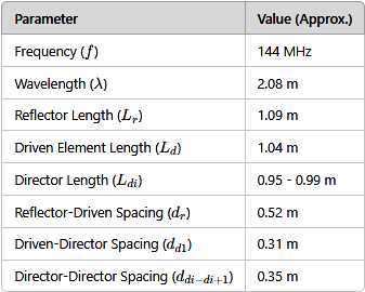
Example: 3-Element, 144 MHz Yagi-Uda Antenna
These calculations
can be scaled to different frequencies by adjusting the wavelength (\(\lambda =
c/f\)) and recalculating lengths and spacings.
Now, let's outline the equations and a table for designing a Yagi-Uda antenna.
An Internet search shows slight variations on the formulas based on personal preferences
and parasitic effects, presence of booms and masts, terrain, mounting configurations,
nearby conductive structures (including other antennas), etc..
Key Equations for Design:
1. Element Lengths:
- Reflector length (Lr): 5% longer than the driven element.

- Driven element length (Ld): Calculated as half the wavelength.

- Director lengths (Ldi): Typically 5-10% shorter than the driven element.
Ldi = 0.9 - 0.96 x Ld
2. Element Spacing:
- Reflector to driven element spacing(dr): 0.2λ
- 0.25λ
- Driven element to first director spacing (dd1):
0.1λ - 0.2λ
- Between directors(ddi-[di+1]):
0.15λ - 0.35λ
3. Gain (Approximate):
For
n directors: G(dB) ≈
10 log10 (1+2n)
4. Input Impedance:
The impedance
Zin depends on the matching network, typically:
Zin = 50 Ω
or 75 Ω
In practical Yagi-Uda antenna designs, real-world factors such as parasitic capacitance
and inductance introduce deviations from the ideal theoretical equations for element
lengths and spacings. These non-idealities stem from the physical construction of
the antenna, the materials used, environmental factors, and interactions between
elements. Here's an explanation of their effects and how they are managed in design
and optimization:
Impact of Non-Ideal Capacitance and Inductance
- Parasitic Capacitance:
- Occurs due to the proximity of antenna elements to one another and the boom.
- Creates a capacitive reactance in the elements, effectively shortening their
electrical length compared to the physical length.
- This effect is more pronounced in closely spaced elements, such as the directors.
- Parasitic Inductance:
- Arises from the finite conductivity of the elements and the physical configuration.
- Adds inductive reactance, which can increase the effective electrical length
of an element.
- This is particularly relevant for the reflector and driven element.
- Mutual Coupling:
- The interaction of near-field electromagnetic energy between elements modifies
their resonant behavior.
- Results in shifts in the resonance frequency of each element from its isolated
theoretical value.
- End Effects:
- Near the tips of the elements, current distribution deviates from the ideal
sinusoidal pattern, causing further deviations in resonant length.
AdjAdjusting for Non-Idealities
- Driven Element Tuning:
The resonant frequency of the driven element is sensitive
to parasitic effects. Designers often incorporate a tuning mechanism, such as a
sliding element or an adjustable gamma match, to compensate for impedance mismatches
and resonance shifts.
- Reflector Adjustment:
The reflector element may require fine-tuning in its
length to account for inductive and capacitive effects, ensuring it adequately reflects
energy forward.
- Director Optimization:
Directors, especially multiple ones in an array,
are the most affected by mutual coupling and parasitics. Their lengths and spacings
are often determined iteratively using electromagnetic simulation software.
Techniques for Managing Non-Idealities
- Modeling and Simulation:
- Modern antenna design tools like NEC (Numerical Electromagnetics Code) and HFSS
(High Frequency Structural Simulator) accurately predict parasitic effects.
- These simulations adjust element lengths, spacings, and feed arrangements to
mitigate deviations.
- Practical Design Adjustments:
- Elements are often made slightly adjustable in physical length.
- Insulating materials with low dielectric constants are used to reduce capacitive
loading.
- Rounded or tapered ends are used to mitigate edge effects and stabilize current
distribution.
- Impedance Matching:
- Baluns, matching networks, or gamma/t-match systems help counteract impedance
changes due to parasitics. /li>
- Designers often match the impedance of the antenna to the feedline (e.g., 50
Ω) by compensating for reactances introduced by non-ideal capacitance and inductance.
- Environmental Considerations:
Environmental factors like proximity to the
ground or nearby structures introduce additional capacitance and detune the antenna.
Placement at an optimal height, typically λ/2 or greater, minimizes these effects.
Practical Implications
Non-idealities mean that Yagi- antennas rarely achieve perfect theoretical performance
in terms of gain, bandwidth, or radiation pattern. However, with careful tuning
and the use of modern computational tools, these imperfections can be minimized,
and the antenna can be brought close to its theoretical ideal. This iterative approach
ensures that the final design performs well within the intended frequency range
and environmental conditions.
 This content was generated by primarily
the ChatGPT (OpenAI), and/or
Gemini (Google), and/or
Arya (GabAI), and/or
Grok 3 (x.AI) artificial intelligence (AI) engine.
Some review was performed to help detect and correct any inaccuracies; however,
you are encouraged to verify the information yourself if it will be used for critical
applications. In some cases, multiple solicitations to the AI engine(s) was(were) used to assimilate
final content. Images and external hyperlinks have also been added occasionally.
Courts have ruled that AI-generated content is not subject to copyright restrictions,
but since I modify them, everything here is protected by RF Cafe copyright. Many
of the images are likewise generated and modified. Your use of this data implies
an agreement to hold totally harmless Kirt Blattenberger, RF Cafe, and any and all
of its assigns. Thank you. Here are the major categories. This content was generated by primarily
the ChatGPT (OpenAI), and/or
Gemini (Google), and/or
Arya (GabAI), and/or
Grok 3 (x.AI) artificial intelligence (AI) engine.
Some review was performed to help detect and correct any inaccuracies; however,
you are encouraged to verify the information yourself if it will be used for critical
applications. In some cases, multiple solicitations to the AI engine(s) was(were) used to assimilate
final content. Images and external hyperlinks have also been added occasionally.
Courts have ruled that AI-generated content is not subject to copyright restrictions,
but since I modify them, everything here is protected by RF Cafe copyright. Many
of the images are likewise generated and modified. Your use of this data implies
an agreement to hold totally harmless Kirt Blattenberger, RF Cafe, and any and all
of its assigns. Thank you. Here are the major categories.
Electronics & High Tech
Companies | Electronics &
Tech Publications | Electronics &
Tech Pioneers | Electronics &
Tech Principles |
Tech Standards Groups &
Industry Associations | Societal
Influences on Technology
|


 The
The


