|
 By Kirt Blattenberger,
RF Engineer, RFCafe.com webmaster By Kirt Blattenberger,
RF Engineer, RFCafe.com webmaster
1. Summary
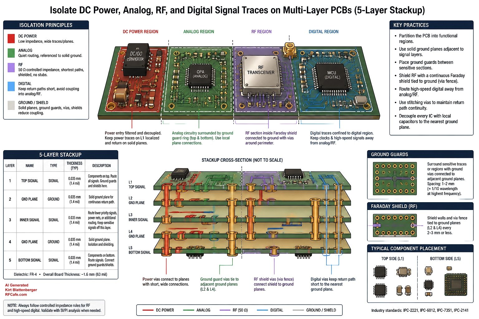
The most effective method for isolating DC power traces, low-frequency analog
signal traces, high-frequency analog signal traces, and digital signal traces on
a multi-layer printed circuit board is not simply to "separate everything with gaps."
The best-practice method is functional partitioning combined with continuous, carefully
assigned reference planes, controlled return-current paths, localized power distribution,
and layer stackup planning. Please note that this is meant to be a guide, not an
absolute plan.
In practical PCB design, signals do not travel only in copper traces. Every signal
current has a corresponding return current, and at higher frequencies that return
current follows the path of lowest impedance, usually directly under or over the
signal trace on the nearest reference plane. Therefore, signal isolation depends
as much on the reference-plane geometry as on trace spacing. A layout that
separates traces but forces their return currents to mix through a shared impedance
can perform worse than a layout with closer traces and a well-controlled return
path.
Electronics & Technology
- See Full List of AI Topics -
For most mixed-signal and RF/digital boards, the strongest general recommendation
is:
- Use a solid, continuous ground reference plane wherever possible.
- Partition the board by function: DC power entry/regulation, low-frequency analog,
high-frequency/RF analog, clocks/high-speed digital, noisy switching power, and
connectors.
- Keep each signal routed over its own uninterrupted reference region.
- Avoid routing high-speed signals across gaps, slots, splits, anti-pads, or plane
changes unless a controlled return-current bridge is provided.
- Use local decoupling, filtering, via
stitching, guarding, controlled impedance,
and, where needed, shielding cans, via fences, stripline layers, or grounded
partitions.
Although many older mixed-signal design discussions recommend "separate analog
and digital grounds," modern high-speed PCB practice generally favors a
single low-impedance ground system with disciplined placement and routing,
rather than indiscriminately splitting ground planes. Split grounds can be useful
in specific systems, but they are also a common cause of electromagnetic interference,
crosstalk, ADC errors, and regulatory test failures when signal traces cross the
split. This principle is emphasized in mixed-signal guidance from Analog Devices
and other industry sources, including Analog Devices' grounding tutorial
MT-031, "Grounding Data Converters and Solving the Mystery of AGND and DGND".
The most robust design approach is to create electrical isolation by
geometry, impedance control, return-path control, filtering, and local referencing,
rather than relying only on copper-plane separation.
2. Key Points
- Return-current control is the central issue. Signal isolation
is ineffective if return currents from digital, analog, RF, and power circuits share
high-impedance paths.
- A continuous ground plane is usually better than multiple split ground
planes. Splitting planes may be appropriate in some low-frequency or safety-isolation
cases, but high-speed and RF traces should not cross splits because return current
is forced to detour, increasing loop area and radiated emissions.
- Functional placement is the first isolation method. Place noisy
digital logic, switching regulators, RF circuits, precision analog circuits, and
power-entry circuits in separate board regions before routing begins.
- Layer stackup matters more than trace separation alone. Signal
layers should be immediately adjacent to solid reference planes. Power and ground
planes should be closely spaced to reduce power-distribution-network impedance.
- Low-frequency analog and high-frequency analog should not be treated
the same. Low-frequency precision analog is often limited by leakage, thermoelectric
effects, ground offsets, and low-frequency noise. High-frequency analog/RF is limited
by impedance discontinuities, coupling, dielectric loss, radiation, and return-current
discontinuity.
- Digital traces must be classified by edge rate, not clock frequency
alone. A slow clock with fast rise/fall times can behave as a high-frequency
signal. High-speed digital lines require controlled impedance and continuous reference
planes.
- DC power traces are not electrically quiet by default. Power
nets carrying switching-regulator ripple, motor current, relay current, LED current,
or pulsed digital load current can inject noise into analog and RF circuits unless
filtered and routed as controlled current loops.
- Do not route sensitive analog traces under digital processors, clocks,
switching inductors, DC/DC converters, or fast memory buses.
- Through-hole parts are useful for connectors, high-voltage spacing,
mechanical strength, and some power components, but they add lead inductance and
consume routing area. Surface-mount parts are preferred for high-frequency
decoupling, RF matching, compact filters, and controlled parasitics.
- Distributed-element techniques become important when physical dimensions
are a meaningful fraction of wavelength. At RF/microwave frequencies, traces,
stubs, vias, and pads behave as transmission-line elements, not ideal wires.
- Shielding is required when layout, filtering, and stackup alone cannot
meet noise, sensitivity, or EMC requirements. Shielding can be implemented
with grounded guard traces, coplanar waveguide ground, via fences, stripline routing,
grounded copper partitions, shield cans, compartmentalized enclosures, or cable
shields.
- Industry standards give design constraints and qualification methods,
but not a single universal layout recipe. Relevant standards include IPC-2221,
IPC-2222, IPC-2152, IPC-6012, IPC-A-600, IPC-A-610, IPC-4101, IPC-4562, IPC-7351,
UL 796, IEC 61000, CISPR 32, FCC Part 15, and, for specialized fields, MIL-STD-461
or automotive EMC standards.
3. Detailed Analysis
3.1 Fundamental Principle: Isolation Means Controlling Current Loops
Every PCB signal path consists of a forward current path and a return current
path. At DC and very low frequency, return current tends to spread through available
copper according to resistance. At higher frequency, return current tends to follow
the path of lowest inductance, usually directly under the signal conductor on the
nearest reference plane. This is the foundation of modern signal-integrity and EMC-aware
PCB design, as discussed in texts such as Henry Ott's
Electromagnetic
Compatibility Engineering and Eric Bogatin's
Signal and Power Integrity - Simplified.
Crosstalk and interference arise from several coupling mechanisms:
| Common-impedance coupling |
Different circuits share the same ground or power impedance |
Precision analog, ADC references, low-level sensors |
Star-like current control, local regulation, low-impedance planes, Kelvin routing,
decoupling |
| Capacitive electric-field coupling |
Voltage transitions couple through parasitic capacitance |
High-impedance analog nodes, reset lines, sensor inputs |
Spacing, guard traces, lower impedance nodes, shielding, slower edges |
| Inductive magnetic-field coupling |
Large di/dt loops induce voltage in nearby loops |
Analog loops, RF front ends, clock circuits |
Minimize loop area, tight forward/return paths, orthogonal routing, plane adjacency |
| Radiated coupling |
Traces, cables, slots, or loops act as antennas |
Entire system, nearby circuits, regulatory emissions |
Continuous reference planes, filtering at I/O, shielding, cable bonding, via
stitching |
| Conducted power-noise coupling |
Load transients and switching regulators modulate supply rails |
PLLs, ADCs, DACs, RF oscillators, op amps |
PDN design, ferrite beads used carefully, LDOs, LC filters, local decoupling |
The practical result is that PCB isolation should be defined as:
Keeping noisy forward and return currents out of sensitive circuit areas,
while keeping all intended signal return paths short, direct, and low impedance.
3.2 Classifying PCB Regions by Signal Reference Type
A mixed-signal PCB should be divided into functional regions before routing.
Typical regions include:
- DC power entry and protection: input connector, fuse, transient
suppressor, reverse-polarity protection, common-mode choke, bulk capacitance.
- Switching power conversion: buck/boost converters, inductors,
switching FETs, rectifiers, current-sense loops, hot loops.
- Quiet power distribution: post-filtered rails, analog LDO outputs,
voltage references, ADC/DAC rails.
- Low-frequency analog: sensors, instrumentation amplifiers,
low-speed op amps, filters, audio, thermocouple, bridge, precision DC measurements.
- High-frequency analog/RF: LNAs, mixers, VCOs, PLLs, RF filters,
impedance-matched traces, antennas, high-speed ADC analog inputs.
- Digital logic: microcontrollers, processors, FPGAs, memory,
buses, clocks, high-speed serial links.
- I/O and cables: connectors, ESD protection, common-mode filtering,
termination, chassis bonding.
The guiding placement rule is:
Place circuits so that their natural current loops stay inside their
own region and do not pass through another region.
For example, the high di/dt loop of a buck regulator should not share copper
with an ADC reference or thermocouple amplifier. Likewise, a processor memory bus
should not route underneath an RF LNA or precision analog input filter.
3.3 Ground Planes: Continuous, Split, Hybrid, and Chassis Ground
3.3.1 The Modern Default: One Continuous Signal Ground Plane
For most multi-layer mixed-signal boards, the most robust starting point is a
single continuous signal ground plane under both analog and digital
circuitry, with careful placement ensuring that digital currents do not flow through
analog regions. Analog Devices makes this point directly in
MT-031: the pins labeled AGND and DGND on a converter often exist to separate
internal chip currents, not necessarily to require two widely separated board grounds.
A continuous plane provides:
- Low return-path impedance.
- Low loop inductance.
- Predictable transmission-line behavior.
- Reduced radiated emissions.
- Reduced sensitivity to plane-resonance and slot-antenna effects.
- Simpler routing of mixed-signal ICs whose analog and digital pins are close
together.
3.3.2 When Split Grounds Are Useful
Ground splits, moats, or isolated ground islands may be useful when there is
a specific reason, such as:
- Safety isolation between primary and secondary circuits in offline power supplies.
- Galvanically isolated communication interfaces.
- High-current motor or solenoid return separated from measurement ground until
a controlled connection point.
- Very low-frequency precision measurements where DC ground voltage drops dominate
and all signals crossing the boundary are carefully controlled.
- RF modules where a local RF ground cavity is stitched and tied to the main ground
at many RF points.
- Medical, intrinsic-safety, or high-voltage circuits requiring regulatory creepage
and clearance.
However, split planes become dangerous when high-speed traces cross them. The
signal current then crosses one path while the return current must detour around
the slot or find a parasitic capacitance path. This increases loop area and can
create strong emissions. If a trace must cross a plane boundary, the designer should
provide a nearby return bridge, such as stitching capacitors, stitching vias to
a continuous reference, or a carefully designed single-point transition, depending
on frequency and isolation requirements.
3.3.3 Analog Ground and Digital Ground on Mixed-Signal ICs
Mixed-signal ICs such as ADCs, DACs, codecs, PLLs, and RF transceivers often
provide separate AGND and DGND pins. In many cases, the recommended layout is:
- Place the IC at the boundary between analog and digital placement regions.
- Route analog pins only into the analog region.
- Route digital pins only into the digital region.
- Connect AGND and DGND to the same low-impedance ground plane near or under the
device, following the manufacturer's layout recommendations.
- Do not route digital traces through the analog region merely because the ground
plane is common.
Texas Instruments, Analog Devices, and other semiconductor vendors commonly publish
evaluation-board layouts and application notes for specific converters. Those device-specific
layout recommendations should override generic rules when they conflict, because
internal chip floorplanning strongly affects optimum grounding.
3.3.4 Chassis Ground, Earth Ground, and Signal Ground
Signal ground and chassis/earth ground should not be treated as the same concept.
Chassis ground is often used for shielding, cable termination, safety, and electrostatic
discharge. Signal ground is the reference for circuits. In EMC-sensitive designs,
cable shields and ESD currents should be bonded to chassis ground near the connector
so that high-current transient energy does not flow through sensitive signal ground.
Relevant EMC test and immunity frameworks include
IEC 61000,
FCC equipment authorization
requirements including Part 15, CISPR publications,
and for military systems
MIL-STD-461.
3.4 Layer Stackup for Isolation
A PCB stackup should be chosen early, before routing, because layer order determines
return-current behavior, impedance, coupling, manufacturability, and emissions.
IPC design standards such as
IPC-2221 and
IPC-2222 provide general
design guidance, while IPC-2152
is commonly used for current-carrying conductor sizing. IPC documents are standards
and are often paywalled, but they are the primary industry references for PCB design
rules.
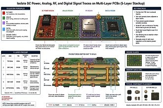
3.4.1 Four-Layer Board Example
| Top |
Components and short critical signals |
Place analog, digital, power, and RF regions physically apart. Route sensitive
traces short. |
| Layer 2 |
Solid ground plane |
Primary reference for top-layer signals. Avoid splits unless absolutely necessary. |
| Layer 3 |
Power plane or mixed power/ground pours† |
Keep power regions separated by function; use local filters and decoupling. |
| Bottom |
Secondary routing, less critical signals, shielding copper |
Route perpendicular to top where possible for LF signals. Maintain reference
continuity. |
† Copper pour (often referred to as a ground pour when connected to the ground net) is an area on a printed circuit board (PCB) layer that is filled with copper, typically used to create a ground plane or balance copper distribution. It is defined by a backoff or stand-off distance, which is a specific clearance maintained between the copper fill and any tracks or pads belonging to a different electrical net.
A four-layer board can work well for moderate-speed mixed-signal systems if Layer
2 is an uninterrupted ground plane. However, four layers may be inadequate for dense
high-speed digital plus RF plus precision analog, because there may not be enough
routing layers with adjacent references.
3.4.2 Six-Layer Board Example
| Top |
Components, RF, short analog, critical digital fanout |
Easy access to parts and tuning components. |
| Layer 2 |
Solid ground plane |
Reference for top layer; EMI control. |
| Layer 3 |
Power distribution |
Close to ground for plane capacitance if dielectric is thin. |
| Layer 4 |
Ground plane or quiet reference plane |
Creates buried stripline reference and isolates power from routing. |
| Layer 5 |
Internal signals, preferably controlled digital or analog |
Referenced to Layer 4 or Layer 6 depending stackup. |
| Bottom |
Components, slow routing, shielding copper |
Useful for secondary components or low-risk traces. |
For isolation, a six-layer stackup with two ground planes is often much better
than a four-layer stackup because it allows signals to be routed adjacent to ground
on both sides of the board.
3.4.3 Eight-Layer Mixed-Signal/RF Example
| Top |
RF, analog components, controlled microstrip, critical short connections |
Grounded coplanar waveguide and via fences may be used for RF. |
| L2 |
Solid ground |
Primary top reference. |
| L3 |
Analog power, RF power, quiet supplies |
Filtered rails; avoid mixing with noisy digital loads. |
| L4 |
Solid ground |
Isolation plane and reference. |
| L5 |
Digital signals, stripline clocks, high-speed buses |
Buried routing reduces radiation. |
| L6 |
Digital power |
Close ground coupling if adjacent to L7. |
| L7 |
Solid ground |
Return plane for bottom and L5/L6. |
| Bottom |
Digital components, slow I/O, test points |
Keep noisy digital away from RF/analog top-side regions where possible. |
This stackup is only an example. Exact construction depends on board thickness,
impedance targets, via technology, component density, and fabrication capability.
3.5 Isolating DC Power Traces and Power Planes
3.5.1 DC Power Is Not Necessarily Quiet
DC rails often carry dynamic currents. A "5 V" rail feeding logic may contain
nanosecond current spikes. A "12 V" rail feeding motors or relays may contain inductive
transients. A switching regulator output may contain ripple, switch-node capacitively
coupled noise, and load-step ringing. Thus DC power should be isolated according
to current type:
- Raw input power: noisy, high-energy, transient-prone.
- Switching regulator hot-loop power: very noisy, high di/dt.
- Digital core power: high transient current.
- Analog power: low noise, often filtered or regulated locally.
- RF power: low noise, requires impedance control and local bypassing.
- Reference power: extremely sensitive, should be isolated from
load currents.
3.5.2 Power Regioning
Best practices include:
- Keep the power-entry section near the power connector.
- Place surge suppression, reverse-polarity protection, EMI filters, and bulk
capacitance at the entry point.
- Keep switching regulators away from low-level analog and RF input areas.
- Minimize the switching regulator "hot loop" formed by input capacitor, switch
FET, diode or synchronous FET, and return path.
- Do not route analog traces under inductors, switch nodes, transformers, or high
di/dt current loops.
- Use separate filtered branches for analog, RF, and digital loads rather than
daisy-chaining quiet loads after noisy loads.
- Use Kelvin sensing for precision voltage feedback and current measurement.
Power-distribution-network design is closely tied to decoupling. Analog
Devices'
MT-101, "Decoupling Techniques" is a widely cited industry tutorial on capacitor
placement and power decoupling.
3.5.3 Power Planes Versus Power Traces
Power planes provide low impedance and help distribute transient current. However,
a large power plane can also spread noise across the board if it is shared by noisy
and sensitive loads. A common strategy is:
- Use solid ground planes as the main low-impedance reference.
- Use power islands or local planes for each rail.
- Feed quiet analog or RF rails through ferrite beads, RC filters, LC filters,
or LDO regulators where appropriate.
- Place decoupling capacitors at the load side of any bead or filter.
- Do not use a ferrite bead as a magic ground or power separator; check its impedance,
DC current rating, saturation behavior, and resonance with capacitors.
3.5.4 Trace Width and Temperature Rise
For power traces, use current, copper weight, allowed temperature rise, voltage
drop, and manufacturability to determine width. The industry reference for current
and temperature rise is IPC-2152,
"Standard for Determining Current-Carrying Capacity in Printed Board Design".
IPC-2221 included older empirical current charts, but IPC-2152 is generally the
more appropriate modern reference.
3.6 Isolating Low-Frequency Analog Signal Traces
3.6.1 Characteristics of Low-Frequency Analog
Low-frequency analog includes DC measurement, audio, sensor signals, bridge circuits,
thermocouples, strain gauges, biomedical inputs, electrochemical sensors, and low-speed
control loops. The relevant problems are often:
- Microvolt or millivolt-level signal amplitudes.
- High source impedance.
- Leakage currents through contamination, flux residue, humidity, or solder mask.
- Ground offsets from load current.
- Thermoelectric junction voltages caused by temperature gradients and dissimilar
metals.
- 1/f noise and low-frequency interference.
- Mains hum pickup at 50/60 Hz and harmonics.
3.6.2 Placement Rules for Low-Frequency Analog
- Place sensors and analog front-end amplifiers close together.
- Keep high-impedance nodes physically short and surrounded by quiet copper.
- Avoid routing near clocks, switching regulators, PWM traces, relays, motors,
and high-current loops.
- Use differential routing for bridge, instrumentation, and low-level sensor signals.
- Use matched trace geometry for differential precision signals when common-mode
rejection is important.
- Use guard rings or driven guards around very high-impedance nodes.
- Keep leakage-sensitive nodes away from board edges, connectors, no-clean flux
residue, and contaminated surfaces.
3.6.3 Grounding for Low-Frequency Analog
Low-frequency analog circuits can be harmed by microvolts of ground error. For
this reason, use:
- Kelvin connections for sense lines and precision references.
- Star-like current routing for heavy load currents, so they
do not flow through analog reference copper.
- Local analog ground region under the analog front end, connected
to the main ground plane with low impedance.
- Separate return paths for high-current loads such as motors,
heaters, LEDs, and relays.
- Input filtering before the first high-gain stage.
Unlike high-speed digital design, where a continuous plane is nearly always needed,
low-frequency precision analog sometimes benefits from carefully controlled star
grounding. The uncertainty is that the best solution depends strongly on source
impedance, bandwidth, enclosure, cabling, ADC architecture, and current levels.
For mixed-signal boards, a continuous ground plane with placement discipline is
still often safer than physical ground splitting.
3.7 Isolating High-Frequency Analog and RF Traces
3.7.1 RF Traces Are Transmission Lines
At high frequencies, PCB traces must be treated as transmission lines. Controlled
impedance, dielectric constant, copper roughness, solder mask, via stubs, pad capacitance,
connector launch geometry, and return-plane continuity all matter. IPC has a high-frequency/microwave
performance specification in
IPC-6018, and material
systems are commonly specified using
IPC-4101 for base materials.
A useful rule of thumb is that transmission-line behavior becomes important when
trace length exceeds approximately one-tenth of the signal wavelength in the dielectric,
or when the edge transition time is short enough that the trace is electrically
long. This is a rule of thumb, not a law; high-Q RF and precision timing applications
may require transmission-line treatment at shorter lengths.
3.7.2 RF Isolation Methods
- Use controlled-impedance microstrip, stripline, or grounded coplanar waveguide.
- Place RF components in a compact chain from input to output.
- Keep RF input and output physically separated to prevent feedback and oscillation.
- Use grounded via fences along RF traces and around RF compartments.
- Use continuous ground under RF traces; never route RF traces over plane splits
or voids.
- Avoid stubs; remove unused branch traces.
- Use back-drilling or blind/buried vias if via stubs are significant at the operating
frequency.
- Use high-Q RF capacitors and inductors with known self-resonant frequency.
- Use shield cans or compartment shields when gain, sensitivity, or EMC requirements
demand it.
3.7.3 Microstrip, Stripline, and Coplanar Waveguide
| Microstrip |
Trace on outer layer over reference plane |
Easy probing and component connection; common for RF |
More radiation and environmental sensitivity than stripline |
| Stripline |
Trace buried between reference planes |
Excellent shielding and predictable return path |
Harder to probe; vias required to reach components |
| Grounded coplanar waveguide |
Trace with ground pours beside it and reference plane below |
Good RF isolation; convenient via fencing |
Requires accurate geometry and fabrication control |
3.7.4 Substrate Choice for RF
Standard FR-4 can be acceptable at lower RF frequencies or for noncritical short
runs, but its dielectric constant and loss tangent vary with resin content, glass
weave, frequency, and supplier. For controlled RF or microwave work, lower-loss
and better-controlled materials are often used, such as Rogers RO4000-series laminates,
Rogers RT/Duroid materials, Isola high-speed laminates, Panasonic Megtron materials,
Taconic laminates, and other low-Dk/low-Df substrates. Manufacturer data should
be used for actual impedance and loss calculations. Rogers provides material data
at Rogers Advanced
Electronics Solutions, and Isola provides laminate data at
Isola Group.
3.8 Isolating Digital Signal Traces
3.8.1 Edge Rate Matters More Than Clock Frequency
Digital signals should be classified by rise/fall time and spectral content,
not just by repetition rate. A 1 MHz square wave with 1 ns edges can create high-frequency
energy well into hundreds of MHz. Therefore, even "low-speed" digital signals can
be EMI sources if their edges are fast.
3.8.2 Digital Placement and Routing
- Place processors, FPGAs, memory, oscillators, and clocks in the digital region.
- Keep clock generators and high-speed oscillators away from analog and RF inputs.
- Route high-speed digital traces over continuous ground planes.
- Do not route high-speed signals across ground-plane splits.
- Use controlled impedance for high-speed buses and serial links.
- Match lengths where timing or skew requirements demand it.
- Use proper termination: series, parallel, Thevenin, AC, or differential termination
as required.
- Keep differential pairs tightly coupled where appropriate and avoid unnecessary
layer changes.
- Provide return vias near signal vias when changing layers.
- Avoid routing digital buses under analog filters, references, VCOs, LNAs, or
crystal oscillators.
3.8.3 Digital Ground Noise
Digital ground noise is caused by simultaneous switching outputs, package inductance,
return-current concentration, and power-distribution impedance. The solution is
not usually a separate digital ground island, but rather:
- Low-inductance decoupling capacitors near IC power pins.
- Short capacitor-to-plane via connections.
- Power and ground planes closely spaced.
- Multiple ground vias for high-current digital ICs.
- Controlled return paths for clocks and high-speed buses.
- Avoiding shared vias or narrow necks in ground return paths.
3.9 Physical Separation and Trace Spacing
Physical spacing reduces capacitive and inductive coupling, but spacing should
be used together with plane control. Common practical rules include:
- Use at least 3W spacing between unrelated moderate-speed traces,
where W is trace width, when space allows.
- Use 5W to 10W spacing between noisy clocks or switch nodes
and sensitive analog traces.
- Increase spacing for high-impedance analog nodes.
- Keep parallel runs short; if traces must cross on adjacent layers, cross at
right angles where practical for low-frequency routing.
- Use grounded guard traces only if they are tied frequently to ground; a long
floating guard can become an antenna.
The "3W rule" is a rule of thumb, not a standard. Accurate prediction of crosstalk
requires field-solving or signal-integrity simulation because coupling depends on
dielectric thickness, reference plane proximity, trace height, length of parallelism,
rise time, impedance, and termination.
3.10 Via Strategy and Return-Path Continuity
Vias are not ideal conductors. They add inductance, capacitance, impedance discontinuity,
and, at high frequency, possible resonant stubs.
Best practices include:
- Place a ground return via near every signal via when the signal changes reference
planes.
- Use multiple ground vias for RF launches, connectors, decoupling capacitors,
and shield-can walls.
- Avoid via stubs on microwave and multi-gigabit links; consider blind vias, buried
vias, or back-drilling.
- Use via stitching along board edges to reduce edge radiation.
- Use via fences around RF or noisy digital regions when isolation is needed.
- Respect fabrication limits for annular ring, aspect ratio, drill size, and plating
reliability.
IPC-A-600, IPC-6012, and related IPC documents define acceptability and performance
requirements for fabricated printed boards. See
IPC-A-600 and
IPC-6012.
3.11 Decoupling, Filtering, and Local Power Isolation
3.11.1 Decoupling Capacitors
Decoupling capacitors provide local transient current and reduce the impedance
between power and ground over a frequency range. Good decoupling practice includes:
- Place capacitors close to IC power pins.
- Use short, wide connections to power and ground planes.
- Use multiple vias for low inductance where needed.
- Choose capacitor values and packages based on impedance versus frequency, not
value alone.
- Account for DC bias derating in ceramic capacitors, especially X5R and X7R MLCCs.
- Use bulk capacitors near power entry and high-load regions.
3.11.2 Ferrite Beads
Ferrite beads can isolate high-frequency noise between power domains, but they
can also create resonant peaks with capacitors. They should be selected based on:
- Impedance versus frequency curve.
- DC current rating.
- DC resistance.
- Saturation behavior.
- Noise spectrum to be attenuated.
- Load transient requirements.
A ferrite bead feeding an analog rail should usually have local decoupling on
both sides, with the load-side capacitors placed close to the analog IC. For sensitive
RF or converter supplies, an LDO or LC filter may be preferable.
3.11.3 Filters at Domain Boundaries
When a signal crosses from a noisy domain to a sensitive domain, consider filtering
at the boundary:
- RC low-pass filters for low-frequency analog inputs.
- Common-mode chokes for differential cables.
- Feedthrough capacitors at shielded compartment walls.
- Pi filters for power entry.
- ESD suppressors near connectors.
- RF attenuators, pads, and matching networks between RF stages.
3.12 Through-Hole, Surface-Mount, and Distributed-Element Components
3.12.1 Through-Hole Components
Through-hole components remain valuable where mechanical strength, high voltage,
high current, field serviceability, or connector durability is important. Examples
include:
- Power connectors.
- Large electrolytic capacitors.
- Relays and transformers.
- High-power resistors.
- Terminal blocks.
- Some RF connectors such as certain SMA or BNC styles.
Limitations include larger parasitic inductance, larger loop area, reduced component
density, and routing blockage due to plated through holes. Through-hole leads are
usually undesirable for very high-frequency decoupling and compact RF matching networks
unless specifically designed for RF use.
3.12.2 Surface-Mount Components
Surface-mount components are generally preferred for high-speed, RF, and compact
mixed-signal work because they offer:
- Lower lead inductance.
- Shorter current loops.
- Better compatibility with automated assembly.
- High component density.
- Availability of precision RF packages.
However, SMD components still have parasitics. A 0402 capacitor may be better
than a 0805 capacitor for high-frequency decoupling due to lower inductance, but
capacitance, voltage rating, DC bias, thermal behavior, assembly yield, and availability
must also be considered.
Footprint design should follow manufacturer recommendations and applicable IPC
footprint standards such as
IPC-7351.
3.12.3 Distributed-Element Components
At RF and microwave frequencies, the PCB itself becomes part of the circuit.
Distributed elements include:
- Microstrip transmission lines.
- Stripline resonators.
- Quarter-wave transformers.
- Open and shorted stubs.
- Interdigital capacitors.
- Hairpin filters.
- Coupled-line directional couplers.
- Printed antennas.
Distributed elements require accurate substrate data, copper thickness, solder-mask
modeling, surface roughness consideration, and manufacturing tolerance analysis.
Their use is common in RF filters, impedance matching, couplers, and antennas, but
they are generally inappropriate for low-frequency analog and ordinary digital circuits.
3.13 Substrate Materials and Copper Systems
3.13.1 Common PCB Materials
| Standard FR-4 |
General digital, low-frequency analog, moderate-speed designs |
Low cost, widely available, mature fabrication |
Loss and dielectric variation at high frequency |
| High-Tg FR-4 |
Lead-free assembly, higher reliability, denser boards |
Better thermal robustness |
Still not necessarily low-loss RF material |
| Low-loss FR-4-like materials |
High-speed digital, moderate RF |
Lower loss than commodity FR-4, compatible processing |
Higher cost; properties vary by product |
| PTFE-based RF laminates |
Microwave, low-loss RF, antennas |
Low loss, stable RF properties |
Higher cost, special fabrication handling |
| Ceramic-filled hydrocarbon laminates |
RF/microwave boards |
Good Dk control and lower loss |
Cost and fabrication considerations |
| Polyimide |
High-temperature, flex, aerospace |
Thermal stability, flex compatibility |
Moisture absorption and cost considerations |
| Metal-core PCB |
LEDs, power electronics, thermal management |
Excellent heat spreading |
Limited routing layers; isolation constraints |
IPC-4101 is a common industry specification for base materials for rigid and
multilayer printed boards. Copper foil properties are addressed in standards such
as IPC-4562.
3.13.2 Dielectric Constant and Loss Tangent
For RF and high-speed digital design, the dielectric constant, Dk, affects impedance
and propagation delay, while dissipation factor, Df, affects insertion loss. Glass
weave can also cause skew in differential pairs. If skew or phase matching is critical,
designers may route at an angle to the weave, use spread-glass materials, or select
materials with tighter dielectric control.
3.13.3 Copper Roughness
At high frequency, skin effect concentrates current near the copper surface.
Copper roughness increases conductor loss. Very high-speed digital and microwave
designs may require low-profile or very-low-profile copper foils. This is a real
effect, but exact impact depends on frequency, trace geometry, copper type, and
laminate system.
3.14 Shielding Between PCB Areas
3.14.1 When Shielding Is Needed
Shielding is needed when ordinary layout isolation is insufficient. Typical cases
include:
- RF receivers with very low-level inputs.
- High-gain analog front ends susceptible to electric-field pickup.
- Oscillators, VCOs, PLLs, and frequency synthesizers.
- Switching power supplies near sensitive analog or RF circuits.
- Products failing radiated or conducted emissions tests.
- Products failing immunity tests such as ESD, EFT, surge, or radiated RF immunity.
- Mixed RF/digital boards where clocks or processors couple into receiver paths.
- Boards connected to long cables that act as antennas.
3.14.2 PCB-Level Shielding Methods
| Ground pour |
Copper pour tied to ground with frequent vias |
General shielding and return control |
Floating copper can resonate; stitch it properly. |
| Guard trace |
Grounded or driven trace beside sensitive node |
High-impedance analog and leakage-sensitive nodes |
Ground guards must be tied frequently; driven guards require stable buffer. |
| Via fence |
Rows of ground vias around RF or noisy region |
RF isolation and cavity boundary control |
Via spacing must be small relative to wavelength. |
| Stripline routing |
Signal buried between ground planes |
High-speed digital and RF needing low radiation |
Harder access for probing and tuning. |
| Shield can |
Soldered metal cover attached to ground ring |
RF sections, oscillators, sensitive receivers |
Requires ground ring, via stitching, rework plan, thermal consideration. |
| Compartment shield |
Metal walls or cans separating board regions |
High-isolation RF and mixed-signal products |
Signals crossing compartments need filtered feedthroughs or controlled transitions. |
| Chassis shield |
Conductive enclosure bonded to PCB ground/chassis points |
System-level EMC |
Poor seams, pigtails, and cable exits can dominate leakage. |
3.14.3 Implementing Shield Cans
For a PCB shield can:
- Define the shielded region during placement, not after routing.
- Place a continuous grounded copper ring around the region.
- Add stitching vias around the ring; for RF, spacing is commonly kept much less
than one-tenth wavelength in the dielectric, and often much tighter in practical
designs.
- Avoid signal traces crossing under the shield wall unless they are intentionally
filtered or referenced.
- Use feedthrough capacitors, pi filters, or controlled transmission-line transitions
for signals entering or leaving the shield.
- Ensure the shield does not short to tall components or detune RF structures.
- Plan for thermal relief, assembly soldering, inspection, and rework.
3.14.4 Guarding Versus Shielding
A guard trace is not the same as a shield. A grounded guard can reduce electric-field
coupling to a sensitive trace. A driven guard, often used around very high-impedance
op-amp inputs or electrometer circuits, is driven to nearly the same voltage as
the sensitive node to reduce leakage current. Driven guards are useful but can oscillate
or add capacitance if poorly implemented.
3.15 Special Considerations for Mixed-Signal ADC and DAC Boards
ADC and DAC boards are among the most common cases where analog, digital, power,
and RF-like behavior coexist. Best practices include:
- Place the converter at the analog/digital boundary.
- Keep the sampling clock clean and isolated from digital data buses.
- Route analog input networks close to the converter input pins.
- Keep voltage reference traces short, quiet, and heavily decoupled according
to datasheet guidance.
- Do not allow digital output currents to flow through analog input return paths.
- Use separate analog and digital supply filtering if recommended by the manufacturer.
- Follow the manufacturer evaluation board layout unless there is a strong reason
not to.
Analog Devices' converter grounding guidance in
MT-031 is especially relevant here. Texas Instruments also publishes extensive
device-specific layout guidance in its data converter and precision analog application
notes at TI Technical Documents.
3.16 Safety Isolation, Creepage, and Clearance
Electrical isolation for noise control is different from safety isolation.
If the PCB includes hazardous voltages, mains input, medical isolation barriers,
or reinforced insulation, the design must satisfy creepage, clearance, dielectric
withstand, pollution degree, material group, and regulatory requirements. Standards
may include IEC 62368-1 for audio/video/ICT equipment, IEC 60601-1 for medical equipment,
IEC 61010-1 for measurement equipment, UL 796 for printed wiring boards, and product-specific
standards.
Do not compromise safety isolation by stitching grounds, placing copper pours,
routing traces, adding test points, or installing shield cans across required isolation
barriers. In such cases, isolated DC/DC converters, digital isolators, optocouplers,
transformers, and controlled Y-capacitors may be required.
3.17 Practical Multi-Layer Layout Workflow
- Define signal classes: raw power, switching power, quiet analog
power, low-frequency analog, RF/high-frequency analog, clocks, high-speed digital,
low-speed digital, chassis/ESD.
- Choose the stackup: ensure every critical signal layer has
an adjacent continuous reference plane. Define impedance targets before layout.
- Partition the board: place regions so natural current flow
does not cross sensitive areas.
- Place connectors first: determine where noise enters and leaves.
Put ESD and EMI parts near connectors.
- Place power circuitry: isolate hot loops, switch nodes, inductors,
and high-current paths.
- Place sensitive analog/RF circuitry: keep inputs short and
quiet. Reserve ground continuity and shielding space.
- Place digital circuitry: keep clocks and high-speed buses away
from analog/RF regions.
- Route critical signals first: RF, clocks, converter inputs,
references, differential pairs, high-speed serial links.
- Control return paths: add return vias near layer transitions;
avoid plane splits and voids.
- Add decoupling and filters: verify capacitor loop inductance
and load-side placement.
- Add stitching and shielding: via fences, edge stitching, shield
rings, guard traces, chassis bonds.
- Review current loops: especially switching regulators, digital
ICs, ADC references, motor drivers, and cable currents.
- Simulate where necessary: impedance, crosstalk, PDN impedance,
RF matching, thermal rise, and EMC risk.
- Prototype and measure: use oscilloscopes, spectrum analyzers,
near-field probes, VNA/TDR where applicable.
3.18 Checklist by Signal Type
| DC power traces |
Voltage drop, ripple, switching noise, load transients, shared impedance |
Separate power regions, local filtering, wide copper, low-impedance planes,
star-like load distribution, Kelvin sense, IPC-2152 sizing |
| Low-frequency analog |
Ground offsets, leakage, hum, capacitive pickup, thermoelectric errors |
Short high-impedance nodes, guard rings, differential routing, quiet ground
region, input filtering, separation from clocks and switchers |
| High-frequency analog/RF |
Impedance discontinuity, radiation, feedback, dielectric loss, via stubs |
Controlled impedance, continuous RF ground, via fences, RF substrate, shield
cans, compact stage placement, avoid stubs |
| Digital signals |
Fast-edge crosstalk, simultaneous switching noise, EMI, return discontinuities |
Continuous ground plane, controlled impedance, termination, return vias, clock
isolation, power decoupling, avoid crossing splits |
4. Open Questions and Debates in the Field
4.1 Split Ground Versus Continuous Ground
This remains one of the most debated PCB layout topics. Older analog practice
often emphasized separate analog and digital grounds connected at one point. Modern
high-speed practice usually emphasizes a continuous ground plane with careful placement.
The correct answer depends on frequency, current magnitude, converter architecture,
cable configuration, and safety requirements. The safest general rule is:
do not split ground planes unless you can explicitly identify the return
currents and prove that no critical signal crosses the split without a return path.
4.2 Ferrite Beads Between Analog and Digital Supplies
Ferrite beads are widely used but sometimes misapplied. They can reduce high-frequency
noise, but they can also resonate with decoupling capacitors and worsen transient
response. Some modern high-speed ICs require very low supply impedance across a
broad band and may not tolerate poorly selected beads. Device datasheets and evaluation-board
layouts should be consulted.
4.3 How Much Shielding Is Enough?
Shielding requirements are difficult to predict analytically because real products
include apertures, seams, cables, connectors, enclosures, and installation variability.
Near-field probing and pre-compliance EMC testing are often necessary. A shield
can may solve one coupling path while leaving cable radiation unchanged.
4.4 FR-4 at RF Frequencies
FR-4 can be adequate for many RF designs at VHF, UHF, and even low microwave
frequencies when traces are short and tolerances are loose. However, for low-loss
filters, antennas, power amplifiers, precision phase matching, or microwave circuits,
controlled RF laminate is usually preferred. The uncertain boundary depends on frequency,
trace length, acceptable loss, impedance tolerance, and production volume.
4.5 Simulation Versus Rules of Thumb
Rules such as 3W spacing, one-tenth wavelength, and "use a solid ground plane"
are useful, but they are approximations. Dense high-speed and RF designs often require
field solvers, signal-integrity simulation, power-integrity simulation, thermal
simulation, and prototype validation.
5. Sources and Standards Cited
- Analog Devices,
MT-031: Grounding Data Converters and Solving the Mystery of AGND and DGND.
- Analog Devices,
MT-101: Decoupling Techniques.
- Texas Instruments, Technical Documents and
Application Notes Library, including data converter, power, and layout guidance.
- Henry W. Ott Consultants,
Electromagnetic
Compatibility Engineering.
- Eric Bogatin,
Signal and Power Integrity - Simplified, Pearson.
- IPC, IPC-2221: Generic
Standard on Printed Board Design.
- IPC, IPC-2222: Sectional
Design Standard for Rigid Organic Printed Boards.
- IPC, IPC-2152: Standard
for Determining Current-Carrying Capacity in Printed Board Design.
- IPC, IPC-4101: Specification
for Base Materials for Rigid and Multilayer Printed Boards.
- IPC, IPC-4562: Metal Foil
for Printed Board Applications.
- IPC, IPC-6012: Qualification
and Performance Specification for Rigid Printed Boards.
- IPC, IPC-6018: Qualification
and Performance Specification for High Frequency Printed Boards.
- IPC, IPC-A-600: Acceptability
of Printed Boards.
- IPC, IPC-A-610: Acceptability
of Electronic Assemblies.
- IPC, IPC-7351: Generic
Requirements for Surface Mount Design and Land Pattern Standard.
- IEC, Electromagnetic Compatibility standards
overview, including IEC 61000 series.
- FCC, Equipment
Authorization and FCC Part 15 compliance information.
- CISPR, International Special Committee on Radio
Interference.
- Defense Logistics Agency,
MIL-STD-461
electromagnetic interference characteristics requirements.
- Rogers Corporation,
Advanced Electronics
Solutions laminate data.
- Isola Group, PCB laminate and prepreg
material data.
- UL,
Printed wiring board testing and certification, including UL 796 context.
Conclusion
The most effective PCB isolation strategy is a system-level method: partition
by function, route with continuous reference planes, keep return currents local,
isolate power domains with filtering and local regulation, use controlled impedance
for high-frequency paths, and add shielding only where electromagnetic coupling
requires it. Ground layers should be placed judiciously not by randomly
splitting them, but by ensuring that each signal type has an uninterrupted, low-impedance
reference path and that noisy currents do not flow through sensitive regions.
For ordinary multi-layer mixed-signal boards, the preferred starting point is
one or more solid ground planes, not multiple disconnected grounds.
For precision analog, RF, high-speed digital, and power electronics, isolation must
be engineered through placement, stackup, routing geometry, filtering, decoupling,
via strategy, materials, and verification. Safety isolation and regulatory EMC requirements
must be handled separately and according to applicable standards.
 This content was generated primarily with
the assistance of ChatGPT (OpenAI), and/or
Gemini (Google), and/or
Arya (GabAI), and/or Grok
(x.AI), and/or DeepSeek artificial intelligence
(AI) engines. Review was performed to help detect and correct any inaccuracies;
however, you are encouraged to verify the information yourself if it will be used
for critical applications. In all cases, multiple solicitations to the AI engine(s)
was(were) used to assimilate final content. Images and external hyperlinks have
also been added occasionally - especially on extensive treatises. Courts have ruled
that AI-generated content is not subject to copyright restrictions, but since I
modify them, everything here is protected by RF Cafe copyright. Many of the images
are likewise generated and modified. Your use of this data implies an agreement
to hold totally harmless Kirt Blattenberger, RF Cafe, and any and all of its assigns.
Thank you. Here is Gab AI in an iFrame. This content was generated primarily with
the assistance of ChatGPT (OpenAI), and/or
Gemini (Google), and/or
Arya (GabAI), and/or Grok
(x.AI), and/or DeepSeek artificial intelligence
(AI) engines. Review was performed to help detect and correct any inaccuracies;
however, you are encouraged to verify the information yourself if it will be used
for critical applications. In all cases, multiple solicitations to the AI engine(s)
was(were) used to assimilate final content. Images and external hyperlinks have
also been added occasionally - especially on extensive treatises. Courts have ruled
that AI-generated content is not subject to copyright restrictions, but since I
modify them, everything here is protected by RF Cafe copyright. Many of the images
are likewise generated and modified. Your use of this data implies an agreement
to hold totally harmless Kirt Blattenberger, RF Cafe, and any and all of its assigns.
Thank you. Here is Gab AI in an iFrame.
Electronics & High Tech
Companies | Electronics &
Tech Publications | Electronics &
Tech Pioneers | Electronics &
Tech Principles |
Tech Standards Groups &
Industry Associations | Societal
Influences on Technology
|